Next: 5. Technology Up: Fabrication and characterization of Previous: 3. III-V compound semiconductor Contents
Atomic Force Microscopy technique provides three-dimensional
surface topographies at nm resolution of a wide range of solid
materials (conducting, insulating, magnetic). The basic principle
is simple: a sharp tip scans the sample surface detecting the
topography. Typical
![]() tips have a
curvature radius of 10-15 nm and opening angle of about
tips have a
curvature radius of 10-15 nm and opening angle of about ![]() . When the tip is brought very near to the surface to
be analyzed, it undergoes attractive or repulsive forces. The
cantilever, on which the tip is located, is deflected. An optical
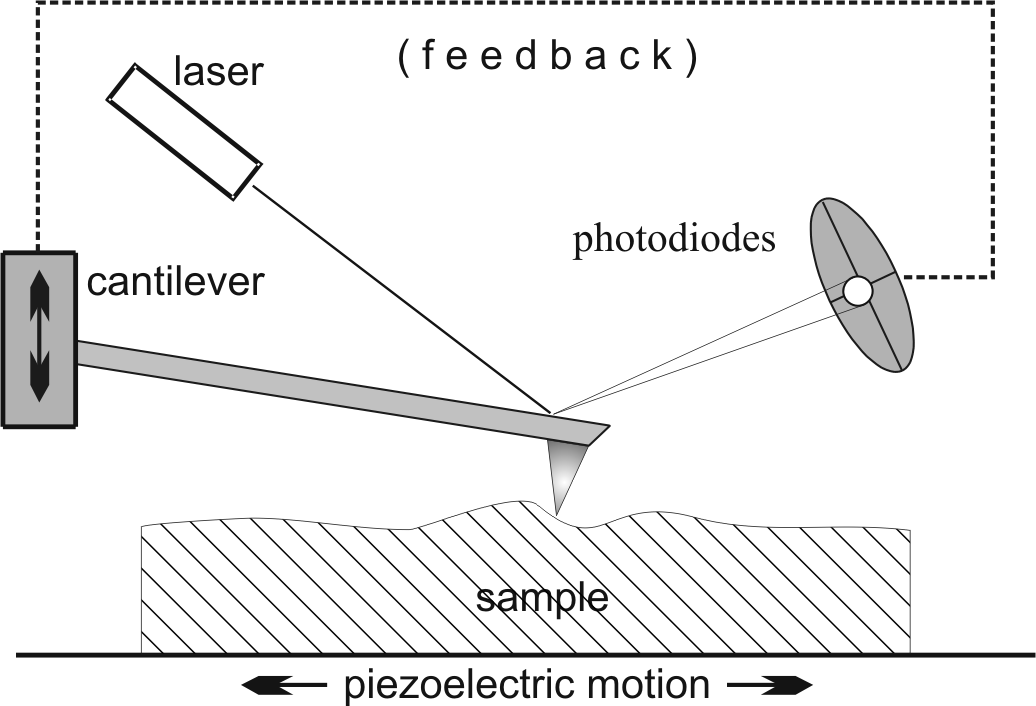
amplification system measures the tip movements. Figure
4.1 shows the system working principle: a laser
beam points on the cantilever and four photodiodes in a cross
configuration detect the reflected beam. While the sample is
scanned, the tip-sample interaction is kept constant by feedback.
. When the tip is brought very near to the surface to
be analyzed, it undergoes attractive or repulsive forces. The
cantilever, on which the tip is located, is deflected. An optical
amplification system measures the tip movements. Figure
4.1 shows the system working principle: a laser
beam points on the cantilever and four photodiodes in a cross
configuration detect the reflected beam. While the sample is
scanned, the tip-sample interaction is kept constant by feedback.
|
Atomic Force Microscope has gone through many modifications for specific application requirements. There are several AFM operating modes: contact mode, tapping mode, phase imaging mode...
The first and foremost mode of operation, the contact
mode, is very similar to a profilometer: the tip-sample forces
are maintained at a constant level and with
piezoelectric motion, the surface is scanned by the tip.
The tapping mode, belongs to a family of AC modes, which
refers to the use of an oscillating cantilever. The tip
intermittently touches or taps the surface. The
natural resonance frequency is shifted by the tip-sample force.
The shift is proportional to the second derivative of the
corresponding potential. This information is then converted in a
topographical image of the surface. In order to filter out the
thermal noise, a lock-in amplification is introduced and a more
stable detection is
allowed.
In phase imaging mode, the phase shift of the oscillating
cantilever relative to the driving signal is measured. This phase
shift can be correlated with specific material properties, which
affect the tip/sample interaction.
The forces acting between the tip and the surface are of different
nature and depend on the tip-sample distance. The first
interaction is the electrostatic force. It begins at
![]() and may be either attractive or repulsive
depending on the material. At
and may be either attractive or repulsive
depending on the material. At
![]() , surface
tension effects result from the presence of condensed water vapor
at the surface. The tip is pulled down toward the sample surface
with attractive force up to
, surface
tension effects result from the presence of condensed water vapor
at the surface. The tip is pulled down toward the sample surface
with attractive force up to
![]() . Van Der Waals
forces appear at the angstrom level above the surface: the atoms
in the tip and sample undergo a weak attraction. Coming even
closer, electron shells from atoms on both tip and sample repulse
one another, preventing further intrusion by one material into the
other (Coulomb forces, contact mode). Pressure exerted
beyond this level leads to mechanical distortion and the tip or
the sample may be damaged.
. Van Der Waals
forces appear at the angstrom level above the surface: the atoms
in the tip and sample undergo a weak attraction. Coming even
closer, electron shells from atoms on both tip and sample repulse
one another, preventing further intrusion by one material into the
other (Coulomb forces, contact mode). Pressure exerted
beyond this level leads to mechanical distortion and the tip or
the sample may be damaged.
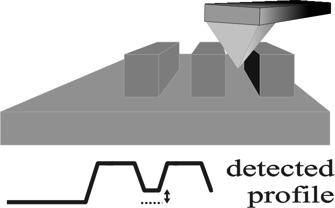
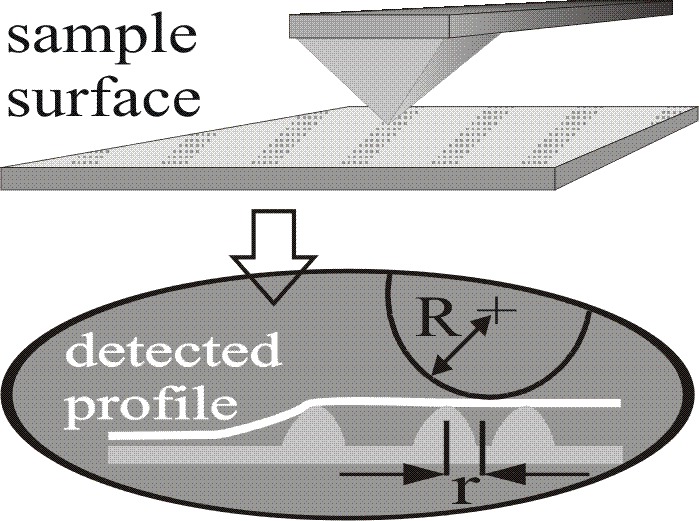
The actual sharpness of a tip influences directly its ability to resolve surface features. Moreover, certain tip damages (e.g. double-pointed and cracked tips) occur very often. In Fig. 4.2, the tip-sample geometry and interactions are considered. One obvious surface limitation is caused by deep grooves (Fig. 4.2(a)): the tip is not long enough, or thin enough, to reach the bottom of a recess. Furthermore, the tip cannot detect walls of the sample with an angle steeper than itself.
 []
[] |
After the air is pumped out from the column, an electron gun (at
the top) emits a beam of high energy electrons. Four different
sources can be used [Was03]: tungsten filament, ![]() crystal tip, Schottky emitter and the cold field emitter. In
ultra-high vacuum conditions (
crystal tip, Schottky emitter and the cold field emitter. In
ultra-high vacuum conditions (![]() mbar), the best beam
properties are supplied by cold field emitter. Schottky emitter is
a good compromise between performance and costs.
mbar), the best beam
properties are supplied by cold field emitter. Schottky emitter is
a good compromise between performance and costs.
The electron beam travels downward through a series of magnetic lenses designed to focus the electrons to a very fine spot. Near the bottom, a set of scanning coils deflect the focused beam back and forth across the specimen, row by row. The SEM images are normally rendered black and white.
Samples have to be prepared carefully to withstand the vacuum inside the microscope. Biological specimens are dried in a special way, which prevents them from shrivelling. Because the SEM illuminates them with electrons, they also have to be made to conduct electricity. Often SEM samples are coated with a very thin layer of gold by sputtering deposition.
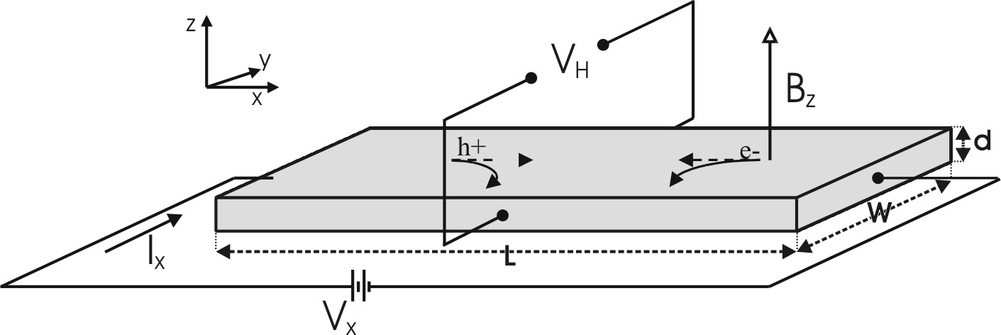
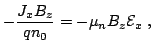
The Hall effect measurement is a widely-used technique to determine electrical properties of semiconductors like majority carrier type, concentration and mobility. The Hall effect is based on the deflection by a magnetic field of moving charged particles.
In Figure 4.3, a rectangular sample has been
considered. A voltage
![]() and a magnetic field
and a magnetic field
![]() are applied. Electrons and holes flowing in the
semiconductor will experience a force, bending their trajectories,
and they will build up on one side of the sample, creating a
potential
are applied. Electrons and holes flowing in the
semiconductor will experience a force, bending their trajectories,
and they will build up on one side of the sample, creating a
potential
![]() across it (the so-called Hall
voltage). Assuming that all the conduction electrons have the
same drift velocity
across it (the so-called Hall
voltage). Assuming that all the conduction electrons have the
same drift velocity
![]() and the same
relaxation time
and the same
relaxation time ![]() , the resulting Lorentz force acting on
any electron is given by:
, the resulting Lorentz force acting on
any electron is given by:
where
![]() is the mobility.
Considering
is the mobility.
Considering
![]() and
and
![]() , the vector
equation 4.4 can be written as two scalar equations:
, the vector
equation 4.4 can be written as two scalar equations:
where
![]() is the conductivity and
relation 4.5 is just the Ohm's law. Equation
4.6 expresses the fact that, along the
is the conductivity and
relation 4.5 is just the Ohm's law. Equation
4.6 expresses the fact that, along the ![]() direction, the force on one electron due to the magnetic field
(
direction, the force on one electron due to the magnetic field
(
![]() ) is balanced by a force
(
) is balanced by a force
(
![]() ) due to the Hall field. (Eq. (4.6))
is generally written as
) due to the Hall field. (Eq. (4.6))
is generally written as
where
![]() is called the Hall
constant. For a p-type semiconductor, it can be shown that
is called the Hall
constant. For a p-type semiconductor, it can be shown that
| (4.8) |
with
![]() , where
, where ![]() is the
equilibrium concentration of holes in the sample. It is thus seen
that
is the
equilibrium concentration of holes in the sample. It is thus seen
that ![]() has a negative sign for electrons and a positive sign
for holes.
has a negative sign for electrons and a positive sign
for holes.
From 4.7, for a rectangular bar like in Fig. 4.3, the Hall constant and the Hall mobility can be expressed by:
where ![]() is the measured Hall voltage,
is the measured Hall voltage, ![]() is
the applied voltage along the length
is
the applied voltage along the length ![]() , and
, and ![]() is the
current. For a semiconductor with comparable concentrations of
electrons and holes,
is the
current. For a semiconductor with comparable concentrations of
electrons and holes, ![]() is given by
is given by
and for a highly ![]() -doped one to
-doped one to
In these two cases, the measurement of ![]() and
and
![]() determines the majority carrier concentration and the
mobility, respectively.
determines the majority carrier concentration and the
mobility, respectively.
The simplest arrangement for measuring the Hall voltage is the
rectangular geometry shown in Fig. 4.3, but a
number of spurious voltages is included in this measurement. All
these spurious voltages are eliminated if four readings are taken
by reversing the direction of the bias current ![]() and the
magnetic flux
and the
magnetic flux ![]() . The true Hall voltage is then obtained by
taking the average of the four readings. The contacts used for
measuring the Hall voltage in Fig. 4.3 should be
infinitesimally small, so that they do not distort the current
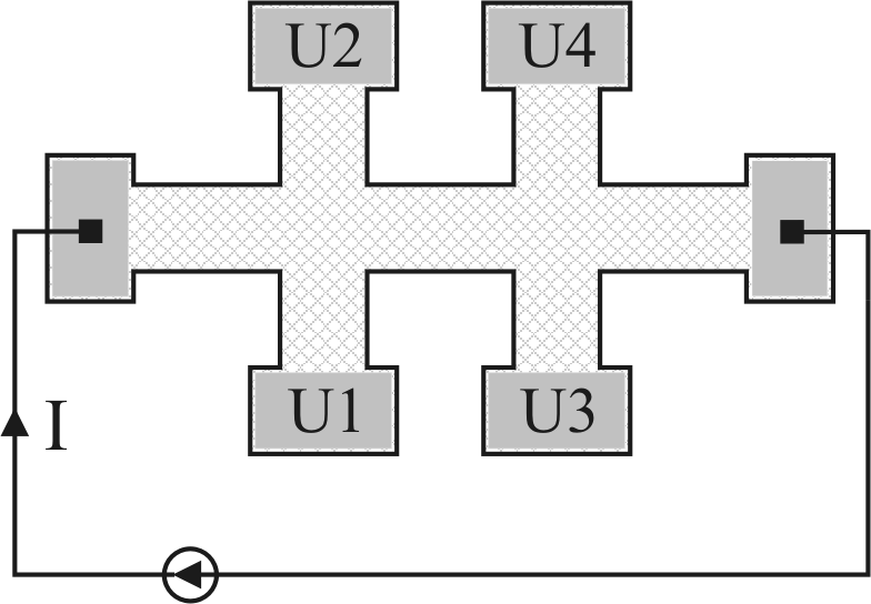
flow. The bridge shaped samples shown in Fig. 4.4(a)
are often used to reduce the distortion of the current. The ears
on the pattern allow a large area to be used for contacting the
sample without a severe distortion of current flowing through the
specimen. The Hall voltage is measured between contacts 1 and 2,
and then between 3 and 4. The average is taken as a final value.
. The true Hall voltage is then obtained by
taking the average of the four readings. The contacts used for
measuring the Hall voltage in Fig. 4.3 should be
infinitesimally small, so that they do not distort the current
flow. The bridge shaped samples shown in Fig. 4.4(a)
are often used to reduce the distortion of the current. The ears
on the pattern allow a large area to be used for contacting the
sample without a severe distortion of current flowing through the
specimen. The Hall voltage is measured between contacts 1 and 2,
and then between 3 and 4. The average is taken as a final value.
 [Van der Pauw arrangement for an arbitrary shaped sample.]
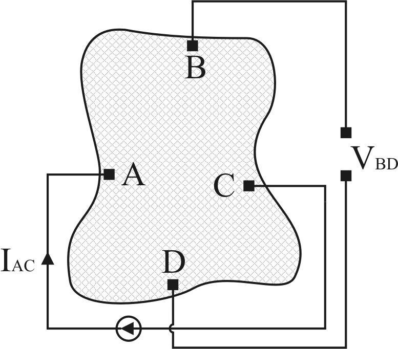 |
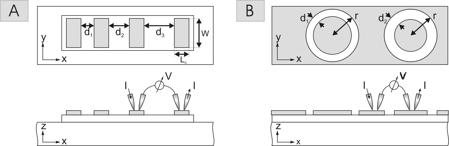
In some cases, it may not be convenient to cut the specimen in the
form of a rectangular bar. Van der Pauw [vdP58] suggested an
interesting method, using an arbitrary shaped thin-flat sample.
The above sample (simply connected, i.e., no holes or
nonconducting islands or inclusions), contains four very small
ohmic contacts placed on the sample periphery (preferably in the
corners). In presence of a normal magnetic field to the sample
surface, a current ![]() is established between two opposite
contacts (a and c), and the voltage is measured between the other
ones (b and d), as shown in Figure 4.4(b).
is established between two opposite
contacts (a and c), and the voltage is measured between the other
ones (b and d), as shown in Figure 4.4(b).
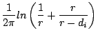
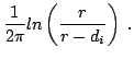
The resistance, defined as:
 |
(4.14) |
A different way to determine the background concentration ![]() of carriers in a semiconductor, is the capacitance-voltage (C-V)
measurement. The C-V method relies on the fact that the width of a
reverse biased space charge region of a junction depends on the
applied voltage. The space charge
of carriers in a semiconductor, is the capacitance-voltage (C-V)
measurement. The C-V method relies on the fact that the width of a
reverse biased space charge region of a junction depends on the
applied voltage. The space charge ![]() per unit area of the
semiconductor junction under an applied bias V is:
per unit area of the
semiconductor junction under an applied bias V is:
In the case of uniform doping concentration, ![]() is
constant within the depletion region and a strait line should be
obtained by plotting
is
constant within the depletion region and a strait line should be
obtained by plotting ![]() versus V. The intercept on the X-axis
of the line represents
versus V. The intercept on the X-axis
of the line represents ![]() , the built-in potential4.1. If
, the built-in potential4.1. If
![]() is not constant, the doping profile can be determined from
the slope of the curve and equation 4.20.
is not constant, the doping profile can be determined from
the slope of the curve and equation 4.20.
| (4.23) | |||
| (4.24) |
 |
(4.25) | ||
 |
(4.26) |
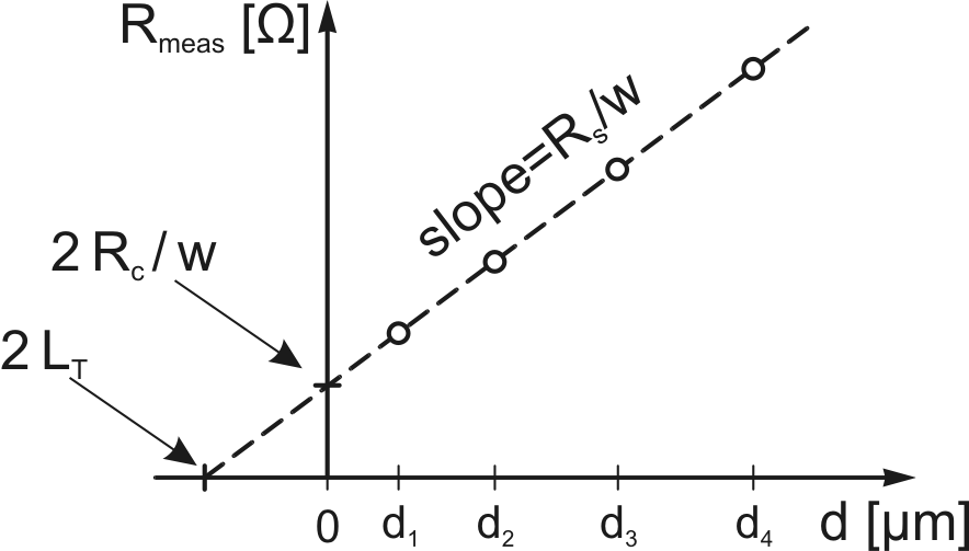
In Fig. 4.6, the measured resistances are
plotted as a function of the distance ![]() . Fitting
Eq. (4.22), the values of
. Fitting
Eq. (4.22), the values of ![]() and
and ![]() can be obtained.
can be obtained.
 |
(4.27) |
 |
(4.28) |
|
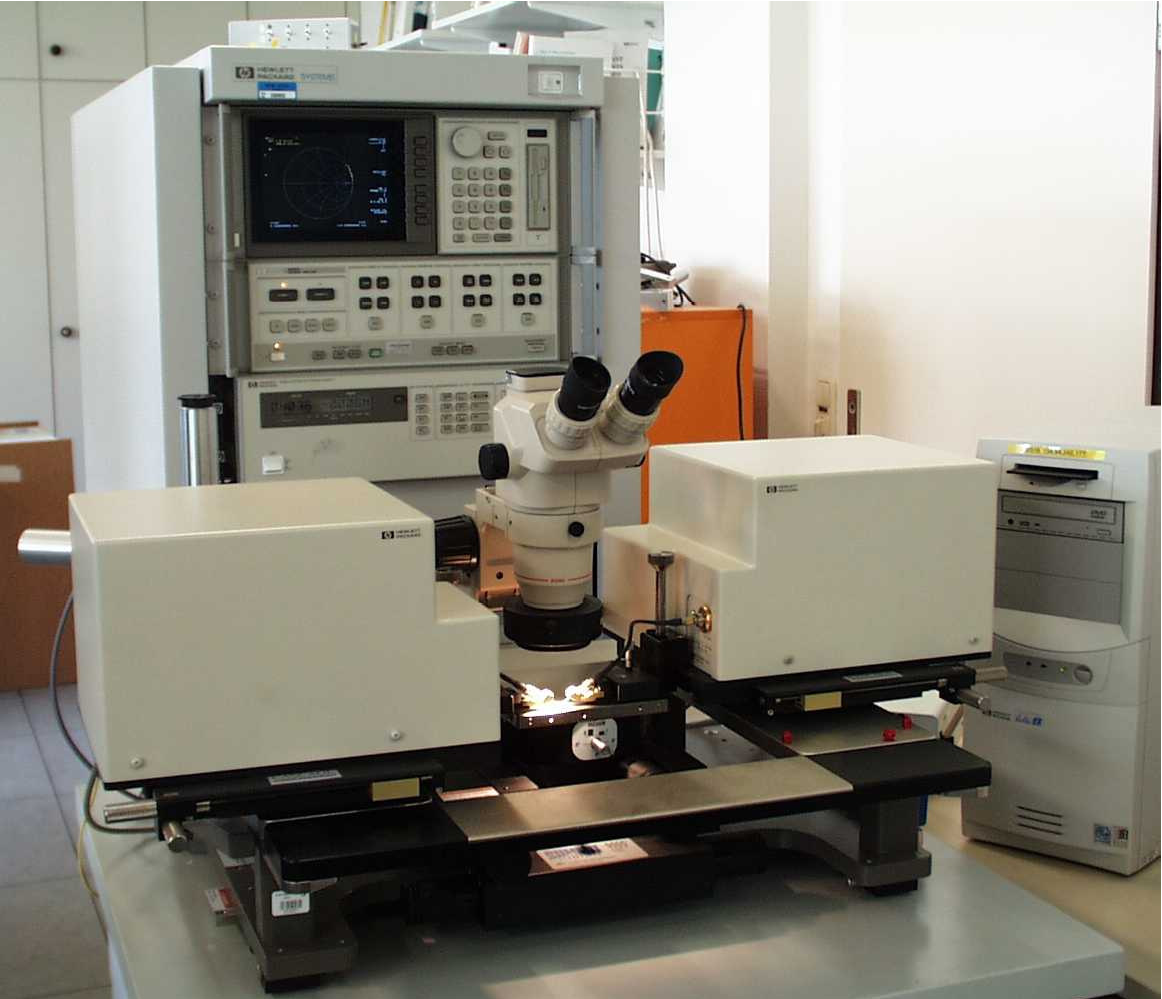
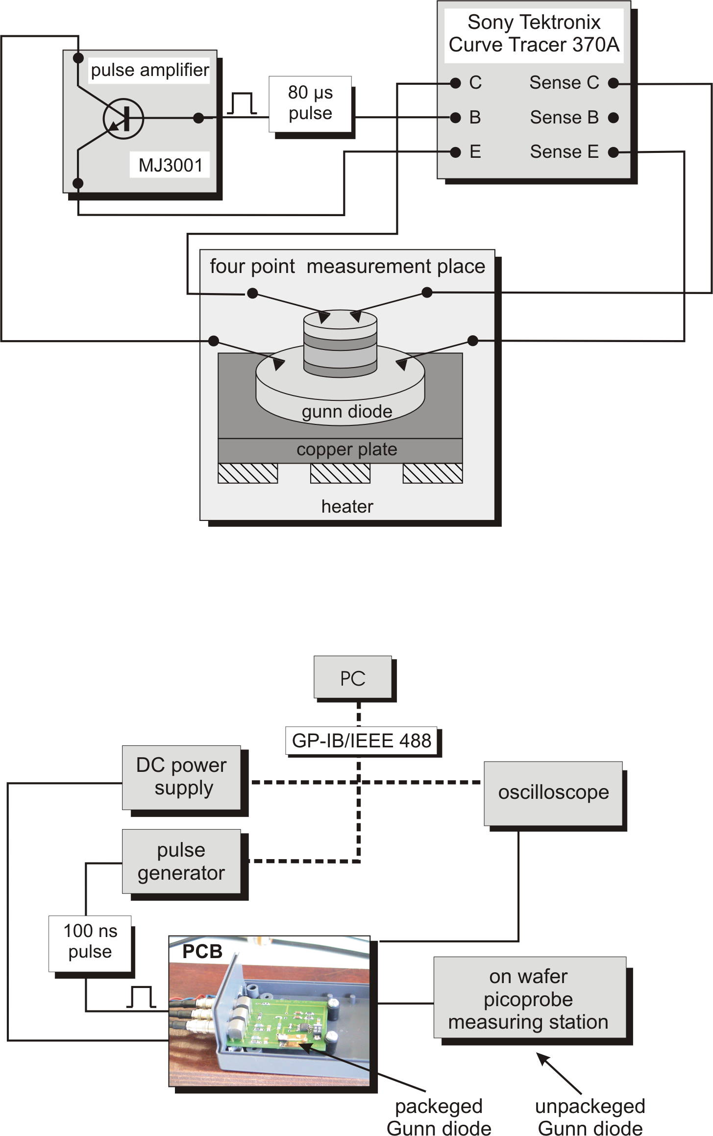
The study of the breakthrough voltage without damaging the Gunn
diode requires DC measurements with very short pulses (
![]() ). Moreover, with different pulse length, the
influence of the diode selfheating on the I-V characteristics can
be determined. For these two reasons, a
). Moreover, with different pulse length, the
influence of the diode selfheating on the I-V characteristics can
be determined. For these two reasons, a
![]() measurement setup has been designed and realized [Pro04]. The
principle scheme of the measurement set-up is presented in
Fig. 4.7(bottom).
measurement setup has been designed and realized [Pro04]. The
principle scheme of the measurement set-up is presented in
Fig. 4.7(bottom).
100 ns pulses are generated from a low-power pulse generator and
are amplified by a custom-designed printed circuit board (PCB),
powered by a computer controlled DC power supply. The pulses are
forwarded to the terminal of the diodes. The short pulse length
requires a special attention in the terminal connection, in order
to avoid line reflections. Therefore, on-wafer measurements are
performed with HF picoprobes. For the packaged diodes, a further
custom adaptor is connected directly to the PCB. The voltage drop
on the diode and on a known serial resistance within the PCB are
measured with a digital oscilloscope. The serial resistance
voltage drop is proportional with the current flowing through the
diode. The sweep range of the voltage pulse can be tuned from
![]() up to
up to
![]() and the current is limited
to
and the current is limited
to
![]() . A HP-VEE program running on a PC controls
the measurements through a IEEE488 interface bus and computes the
diode DC characteristics from the oscilloscope raw data.
. A HP-VEE program running on a PC controls
the measurements through a IEEE488 interface bus and computes the
diode DC characteristics from the oscilloscope raw data.
Temperature dependent measurements have been more complicated and
time consuming: they have required to build a compact custom-made
temperature controller based on a peltier element and a PT100
thermosensor. The temperature is function of the resistance of the
PT100, which is embedded in a flat copper block. The peltier
element cools or heats (depending on the terminal polarity) the
copper block, transferring the heat to or from a big metal
reservoir, kept at room temperature. In the considered setup, the
sample is fixed with vacuum on the copper block and the
temperature can be tuned from 2
![]()
![]() C up to
C up to ![]() C. Lower
temperatures can not be reached because of ice formation and
higher ones could damage the HF picoprobes.
C. Lower
temperatures can not be reached because of ice formation and
higher ones could damage the HF picoprobes.
When making on-wafer measurements, an ongoing concern is how accurate and repeatable are the collected data. The hardware has to be as good as practically possible, balancing performance and costs; error corrections can be an useful tool to improve measurement accuracy. The basic source of measurement errors are:
Before a network analyzer can make error-corrected measurements, the network analyzer systematic errors must be measured and removed. Calibration is the process of quantifying these errors by measuring known precision standards. Three techniques are commonly used to calibrate network analyzers and wafer probing stations:
The LRRM4.2, a variation of LRM, was used for most of the measurements with the HP8510C-XF vector network analyzer in Figure 4.8; it was usually software assisted by WinCal, a program developed by Cascade Microtech, which supplied also the picoprobes and the probing station.
During HF measurements and after data has been collected, it is essential to have an overview over the produced results. The fastest way is to display data with some kind of graphical interfaces (normally integrated in the measurement system or in a software package for computer controlled measurement systems). The most popular diagram for each parameter are:
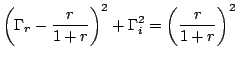
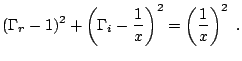
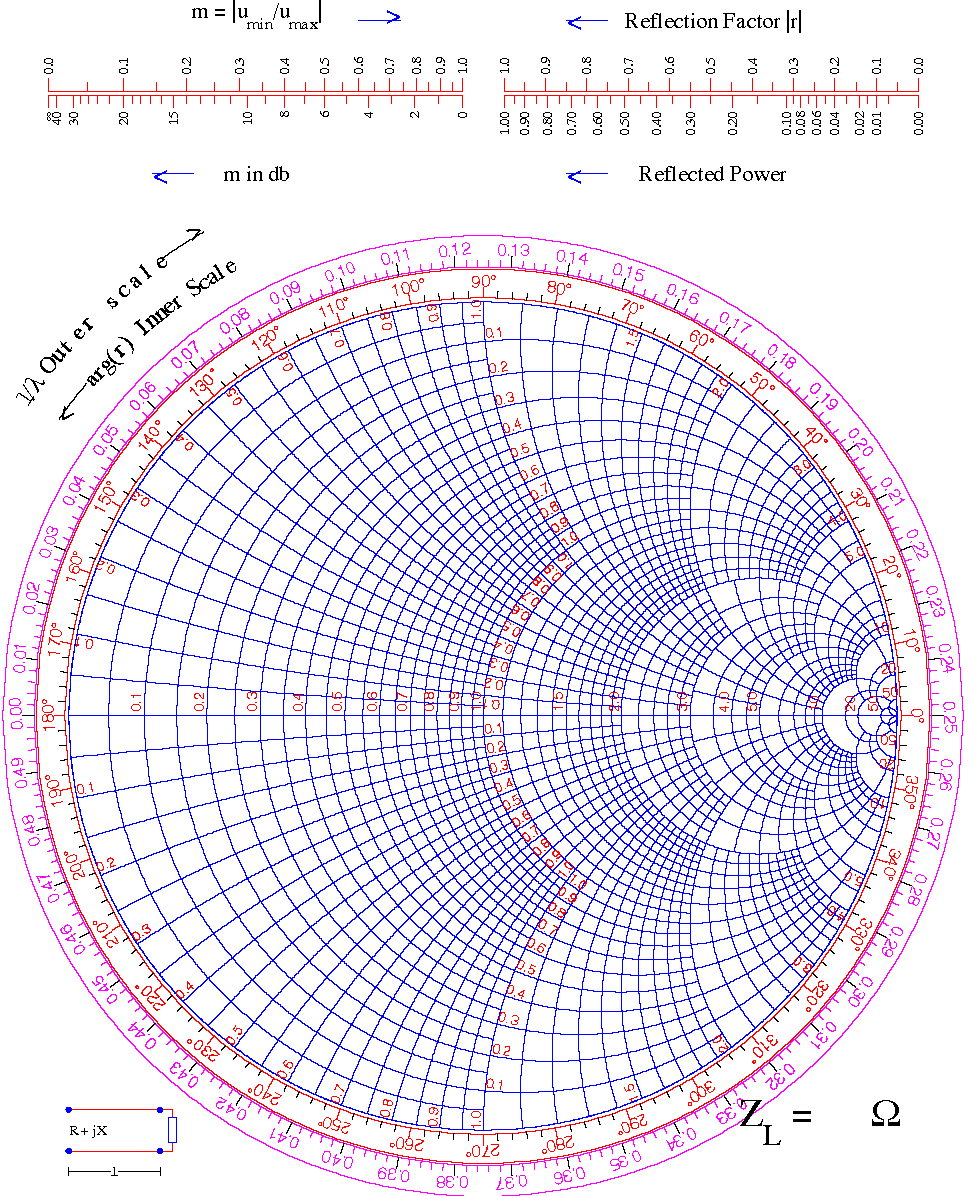
Smith chart represents the standard for
The Smith Chart is derived from the relationship between
complex reflection coefficient ![]() and complex impedance Z.
and complex impedance Z.
Writing the impedance and the reflection coefficient as
function of the real and imaginary components, ![]() and
and
![]() , equation 4.29 is equivalent
with:
, equation 4.29 is equivalent
with:
 |
(4.30) | ||
 |
(4.31) |
To actually see the form of the equations for deriving the Smith Chart, we rearrange the terms to obtain the equations for a set of circles:
From equations 4.32 and 4.33 the Smith Chart can be easily drawn. Some key features of this chart (Fig. 4.9) are listed: