Next: 4. Experimental Methods Up: Fabrication and characterization of Previous: 2. Device Physics / Contents
|
Goldschmidt was the first who created GaAs in 1929. He found that it has a zincblende lattice with a FCC symmetry [Gol29]. Only in 1952, in fact, GaAs has been identified as a semiconductor by Welker (Siemens)3.1. The nature of the bond between gallium and arsine is predominantly covalent. The first device exploiting the direct band-gap of GaAs dates from 1962, when Hall et al. at GE [HFKC62] and Redhiker at al. at MIT Lincoln Laboratory [QRK+62], independently, obtained the first semiconductor laser. In the same year, Gunn (IBM) discovered the transferred electron effect and developed the first solid state microwave oscillator [Gun63].
|
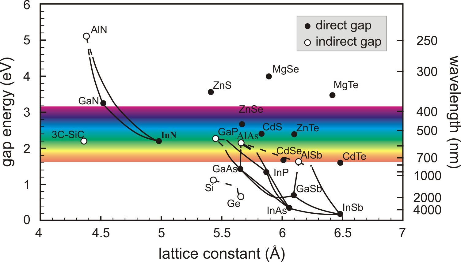
Figure 3.1 shows the energy gaps and the
lattice constants of of the most important elemental and binary
cubic semiconductors. The connecting lines consider the case of
ternary compounds, composed of various ratios of the corresponding
binary materials. The compound
![]() maintains nearly
the same lattice constant with the change of the Al mole fraction.
This property and the related high quality heteroepitaxy have
opened new possibilities for advanced devices like double
heterostructure lasers, high electron mobility transistors and
heterostructure bipolar transistors; to describe the large
possibilities offered by the epitaxial growth using
maintains nearly
the same lattice constant with the change of the Al mole fraction.
This property and the related high quality heteroepitaxy have
opened new possibilities for advanced devices like double
heterostructure lasers, high electron mobility transistors and
heterostructure bipolar transistors; to describe the large
possibilities offered by the epitaxial growth using
![]() , and in general III/V compounds, a new expression
has been coined: bandgap engineering.
, and in general III/V compounds, a new expression
has been coined: bandgap engineering.
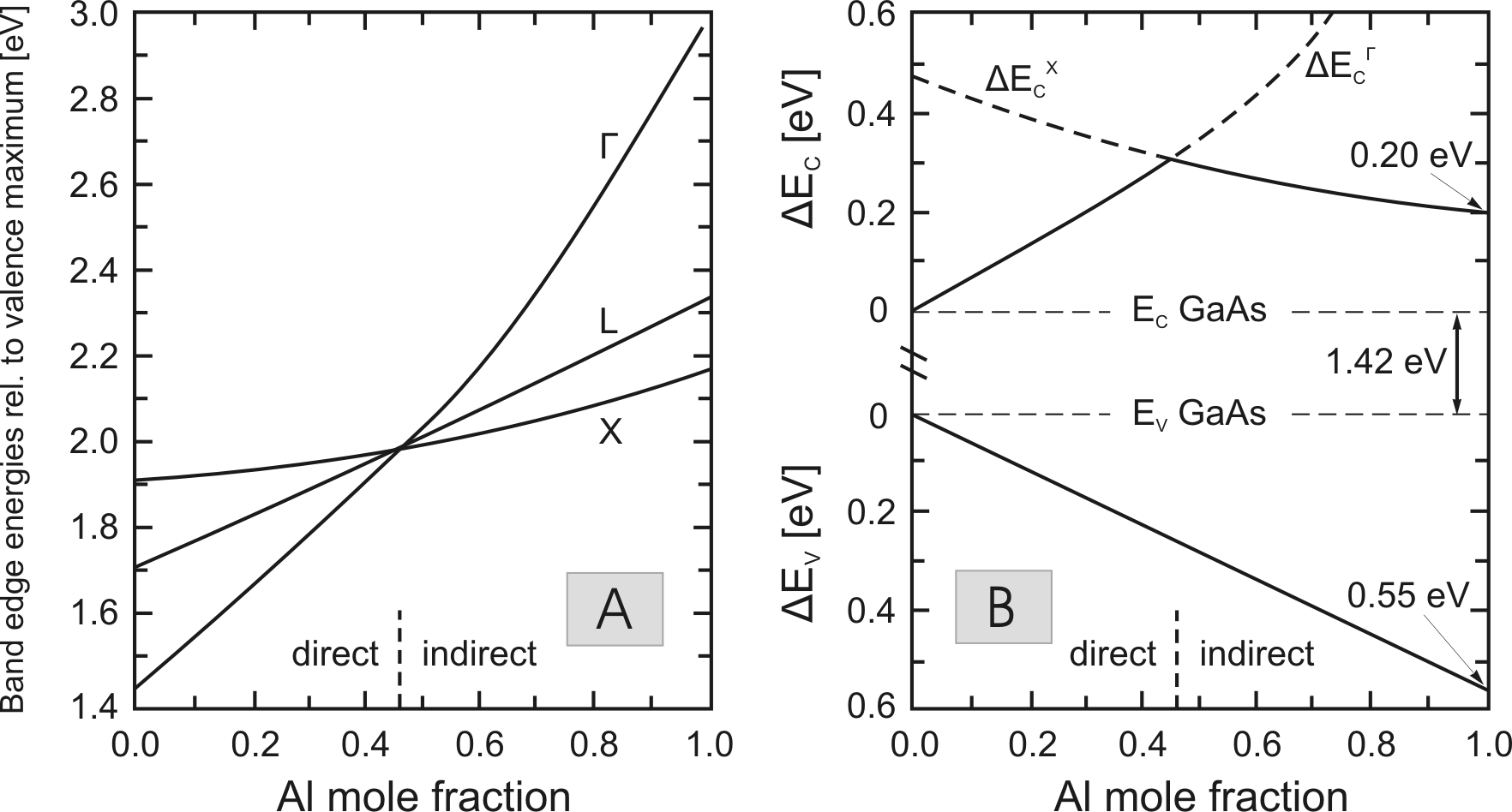
In Fig. 3.2, the bandgap energy of the
![]() material system is plotted versus the Al
concentration in different points of the Brillouin zone. At about
45% Al, the transition between direct and indirect bandgap can be
observed.
material system is plotted versus the Al
concentration in different points of the Brillouin zone. At about
45% Al, the transition between direct and indirect bandgap can be
observed.
|
As in the case of arsenides, between group III - elements and
nitrogen, the nature of the bond is mainly covalent. However, for
the nitrides, the large difference in the electronegativities
causes a strong ionic component, which means very high bonding
energies (AlN 11.5, GaN 8.9 and InN
![]() ) and
consequently excellent thermal and chemical stability. In contrast
to GaAs, the thermodynamically stable phase of these materials is
the hexagonal wurtzite structure,
) and
consequently excellent thermal and chemical stability. In contrast
to GaAs, the thermodynamically stable phase of these materials is
the hexagonal wurtzite structure,
![]() . Beside to
. Beside to
![]() , a metastable
, a metastable
![]() with zincblende
structure exists if very thin layers of GaN and InN are grown on
cubic substrates like GaAs or silicon. The nitride materials with
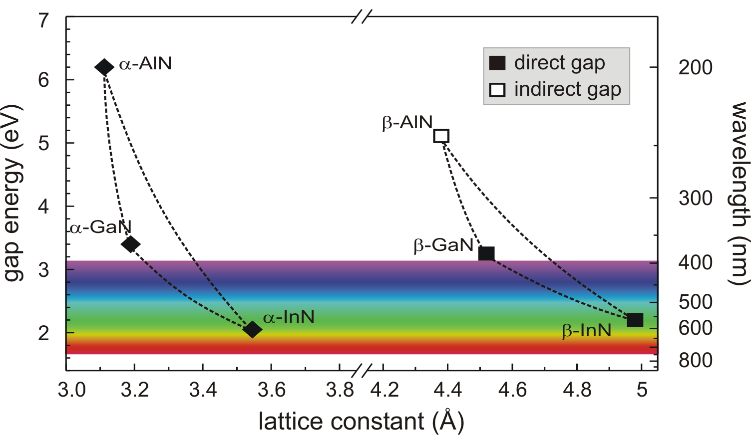
wurtzite structure form an alloy system (InGaN, AlGaN, InAlN),
whose direct bandgaps range from 0.7 to
with zincblende
structure exists if very thin layers of GaN and InN are grown on
cubic substrates like GaAs or silicon. The nitride materials with
wurtzite structure form an alloy system (InGaN, AlGaN, InAlN),
whose direct bandgaps range from 0.7 to
![]() (Fig. 3.3). These give to group III-nitride
unique optical properties, making them suitable for a large
spectrum of optoelectronic applications. Another peculiarity of
group III nitrides, in comparison with arsenides, is the existence
of strong spontaneous and piezoelectric polarization fields. This
property leads to an additional carrier accumulation at the
strained interfaces
(Fig. 3.3). These give to group III-nitride
unique optical properties, making them suitable for a large
spectrum of optoelectronic applications. Another peculiarity of
group III nitrides, in comparison with arsenides, is the existence
of strong spontaneous and piezoelectric polarization fields. This
property leads to an additional carrier accumulation at the
strained interfaces
![]() in 2DEG structures,
enhancing the electron concentrations in GaN HEMTs.
in 2DEG structures,
enhancing the electron concentrations in GaN HEMTs.
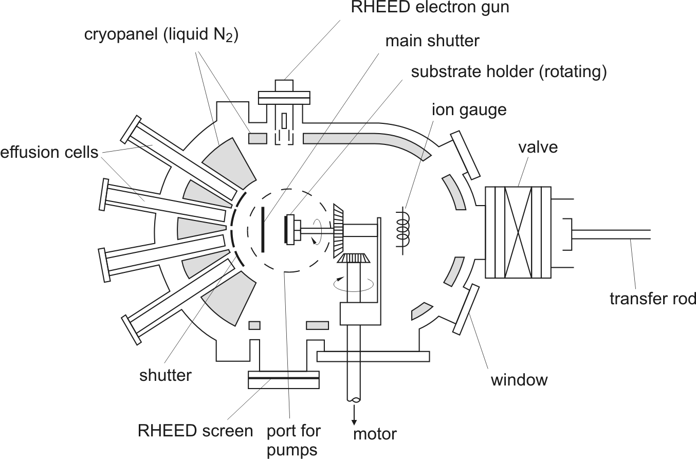
The GaAs Gunn diode structures considered in this thesis have been
grown by molecular-beam epitaxy (MBE) on 2-inch semi-insulating
GaAs substrates in a Varian ModGen II MBE system. The principle
scheme of the MBE growth chamber is shown in
Fig. 3.4. The substrate holder can be heated up
to 900
![]()
![]() C . The source materials Ga, As, In, Al, Si (for
n-doping) and Be (for p-doping) are placed in the effusion cells.
The growth rate can be measured by a RHEED3.2 system and is
controlled by tuning the cells temperature. In order to monitor
the doping levels, calibration samples are periodically grown and
characterized by Hall and CV measurements (sections
4.3 and 4.4).
C . The source materials Ga, As, In, Al, Si (for
n-doping) and Be (for p-doping) are placed in the effusion cells.
The growth rate can be measured by a RHEED3.2 system and is
controlled by tuning the cells temperature. In order to monitor
the doping levels, calibration samples are periodically grown and
characterized by Hall and CV measurements (sections
4.3 and 4.4).
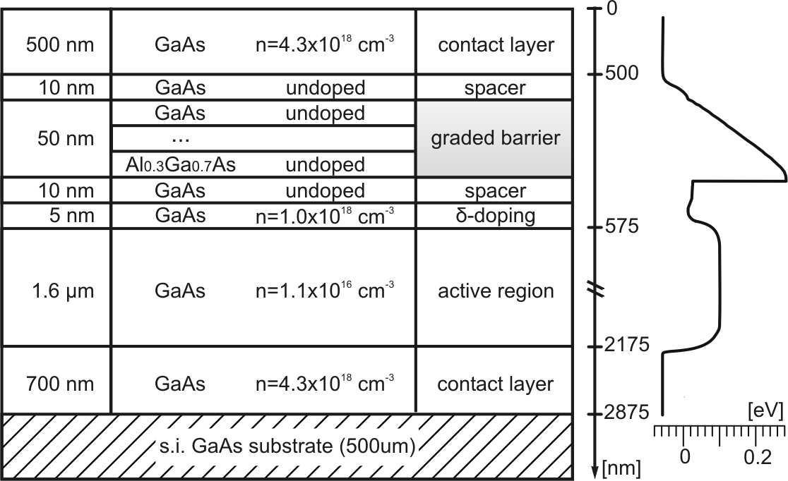
A typical layer sequence of a GaAs Gunn diode with a graded gap
injector is sketched in Fig. 3.5.
It consists mainly of an undoped AlGaAs graded barrier structure
followed by a ![]() doping and a thick low doped GaAs active
region. The grading is linear, starting from 1.7% up to the
maximum Al value. The role of the two
doping and a thick low doped GaAs active
region. The grading is linear, starting from 1.7% up to the
maximum Al value. The role of the two
![]() GaAs
spacers is to avoid doping diffusion in the graded barrier.
GaAs
spacers is to avoid doping diffusion in the graded barrier.
In this work, different structures have been considered:
The first structure (W16016) is mainly used as a reference. Even if the electrical measurements show no hint of a hot electron injector, W16016 allows a comparison with the other structures. Wafers W18006 and W18021, which have the same full-working graded gap injector, were grown to demonstrate the influence of the active region length on the diode high frequency behaviour. Finally, in wafers from W18038 to W18041, the role of the maximum Al content in the injector has been examined.
|
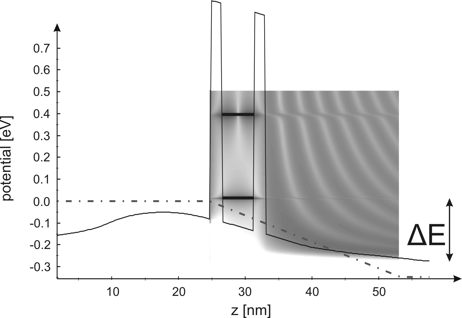
The simulation of the resonant tunneling injector was done with
the software package Wingreen [IM]. This is based on a
self-consistent real-time Green's function approach [Ind99].
A simulation example is shown in Fig. 3.6. The
conduction band and the local density of states of a RTI are
presented for an applied bias voltage. The chosen bias voltage
corresponds to a current density in the range 23-27 ![]() . The
layer structure has to be so that the following condition is
satisfied: the first transmission energy level for the given
current density range has to match the energy difference between
the L- and the
. The
layer structure has to be so that the following condition is
satisfied: the first transmission energy level for the given
current density range has to match the energy difference between
the L- and the ![]() -valley (
-valley (
![]() for GaAs). In order to make the
RTI competitive, a further specification has been defined: the
voltage drop on the RTI for the working current conditions, must
be much lower than the one on the GGI.
for GaAs). In order to make the
RTI competitive, a further specification has been defined: the
voltage drop on the RTI for the working current conditions, must
be much lower than the one on the GGI.
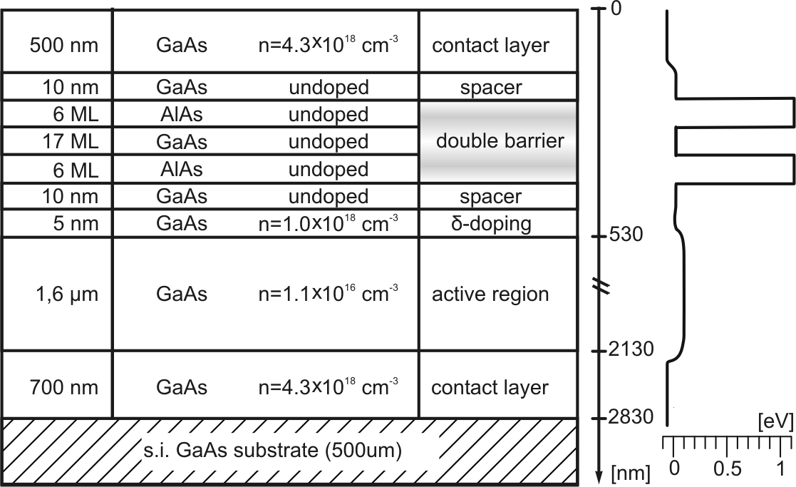
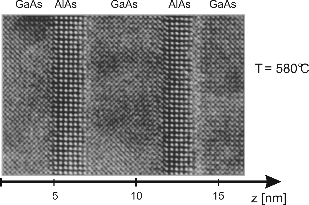
In Fig. 3.7, a typical layer sequence of
the RTI GaAs Gunn diode is presented. The structure is very
similar to that of GGI GaAs Gunn diode: the active region, the
spacers and the ![]() -doping layers have not been changed. The
injector itself is undoped and consists in a sequence of
AlAs/GaAs/AsAs (
-doping layers have not been changed. The
injector itself is undoped and consists in a sequence of
AlAs/GaAs/AsAs (
![]() /
/
![]() /
/
![]() , W18069). A second wafer
has been grown decreasing the AlAs thickness from 6 to
, W18069). A second wafer
has been grown decreasing the AlAs thickness from 6 to
![]() (W18069). The High Resolution Transmission
Electron Microscopy (HRTEM) image illustrates a resonant tunneling
double barrier with
(W18069). The High Resolution Transmission
Electron Microscopy (HRTEM) image illustrates a resonant tunneling
double barrier with
![]() of AlAs. The sample has
been grown at
of AlAs. The sample has
been grown at
![]() C, an optimal temperature
for well defined GaAs/AlAs interfaces [Lan99].
C, an optimal temperature
for well defined GaAs/AlAs interfaces [Lan99].
|
The MOVPE is characterized by large-area growth capability, high
surface mobility of the precursor gaseous molecules, good layer
uniformity and precise control of the epitaxial deposition. These
reasons together with the higher growth rate, made the MOVPE to be
the favourite growth method for industrial purposes. By this
technique, the gas phase growth precursors are transported by a
carrier gas to a heated substrate, where the precursors are
pyrolysed and the nitride film is deposited. The diffusion of the
active materials to the substrate are favored by the depletion at
the surface and the consequent concentration gradient of these
materials in the gas phase, due to their consumption during the
growth. The obtained byproducts are then transported out from the
reactor together with the unused reactants. As group III sources,
trimethylgallium or triethylgallium (-indium,-alluminium) are
used, whereas the common nitrogen source is ammonia (![]() ). The
high thermal stability of
). The
high thermal stability of ![]() , although still low compared to
, although still low compared to
![]() , is one reason to use high substrate temperatures,
typically more than 550
, is one reason to use high substrate temperatures,
typically more than 550![]() C for InN and above 900
C for InN and above 900![]() C
for GaN and AlN. The high growth temperature and thus the high
nitrogen vapor pressure lead to the problem of nitrogen loss from
the nitride film and to carbon contamination from the
decomposition of the organic radical during metalorganic
pyrolysis. The loss of nitrogen is usually alleviated by the use
of high V/III gas ratios during the deposition. The extreme
requirements for the nitride growth have led also to the
development of new MOVPE reactor designs.
C
for GaN and AlN. The high growth temperature and thus the high
nitrogen vapor pressure lead to the problem of nitrogen loss from
the nitride film and to carbon contamination from the
decomposition of the organic radical during metalorganic
pyrolysis. The loss of nitrogen is usually alleviated by the use
of high V/III gas ratios during the deposition. The extreme
requirements for the nitride growth have led also to the
development of new MOVPE reactor designs.
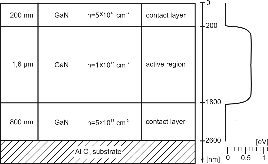
The GaN Gunn diode structures, considered in this thesis, have
been grown by MOVPE in an Aixtron AIX200 reactor on two inch ![]() substrates. Unlike the MBE system, RHEED is not suitable for
in-situ monitoring of the growth rate in the high-pressure
environment like MOVPE. RHEED requires a high electron mean free
path, which can be achieved only in ultra high vacuum conditions.
The growth rate is therefore determined by normalized
reflectometry. A more accurate description of the MOVPE epitaxy
and the experimental setup can be found in [Kal03].
substrates. Unlike the MBE system, RHEED is not suitable for
in-situ monitoring of the growth rate in the high-pressure
environment like MOVPE. RHEED requires a high electron mean free
path, which can be achieved only in ultra high vacuum conditions.
The growth rate is therefore determined by normalized
reflectometry. A more accurate description of the MOVPE epitaxy
and the experimental setup can be found in [Kal03].