Subsections
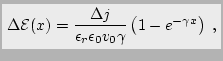
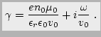
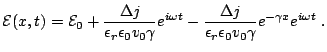
In this chapter an overview of the basic principles behind a Gunn
oscillator is presented. The phenomenon of the bulk negative
conductivity concerning semiconductor with a particular band
structure is explained. Relevance is given to the conditions under
which oscillations, small signal amplification or only pure ohmic
behaviour of the Gunn devices are achieved. A detailed description
of different Gunn injectors will point out the possible device
improvements. Finally the heat-sink issue is explained and a
finite elemente thermal analysis illustrates the best
geometric/material configurations for cooling
Gunn devices.
The Gunn diode, also known as Transferred Electron Device (TED),
is an active two-terminal solid-state device. It is unique in
the sense that its voltage controlled negative differential
resistance is only depending on bulk material properties rather
than a junction or an interface.
The fundamental mechanism, the transferred-electron effect, was
theoretically described by B. K. Ridley and T.B. Watkins in 1961
[RW61]. In 1962, Hilsum predicted the possibility of
transfer-electron amplifiers and oscillators [Hil62]. In
spite of Ridley-Watkins-Hilsum work, the transferred electron
effect was named after an IBM researcher interested in the
response of III-V semiconductors on pulsed voltages, J. B. Gunn.
In 1962, independently Gunn observed a "noisy" resistance,
measured as a function of the voltage, applying
 on a GaAs sample. "Why did the reflected signal from a
50
on a GaAs sample. "Why did the reflected signal from a
50 transmission line, terminated in GaAs sample, produce
several ampere of noise?"
transmission line, terminated in GaAs sample, produce
several ampere of noise?"
With better equipment Gunn detected
regular current oscillations at about 5GHz and applied for a
patent (1963). This spontaneous discovery founded the development
of active-semiconductor devices to replace microwave vacuum tubes.
After publishing his results [Gun63,Gun64,Dun65], many
researchers started studying Gunn diodes.
H. Krömer was the
first to link Gunn oscillations with the transferred-electron
effect in 1964 ([Krö64]). A convincing evidence of such a
correlation was delivered by A. R. Hutson, A. Jayaraman and A. G.
Chynoweth from Bell Labs in 1965. They showed how hydrostatic
pressure could first decrease the threshold field and then
suppress the current oscillations, demonstrating that the Gunn
oscillations are based on the electron transfer from the low- to
the high-energy valley ( and L).
2.1.2 The transferred-electron effect and the domain formation
Figure 2.2:
Crystallographic directions in a zinc-blende crystal.
| 6cm
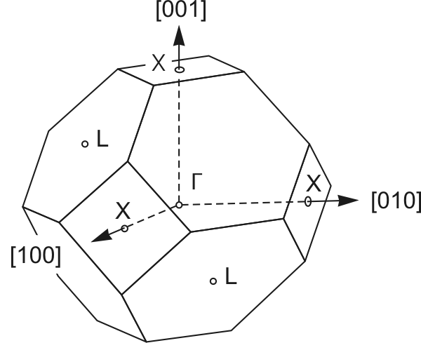 |
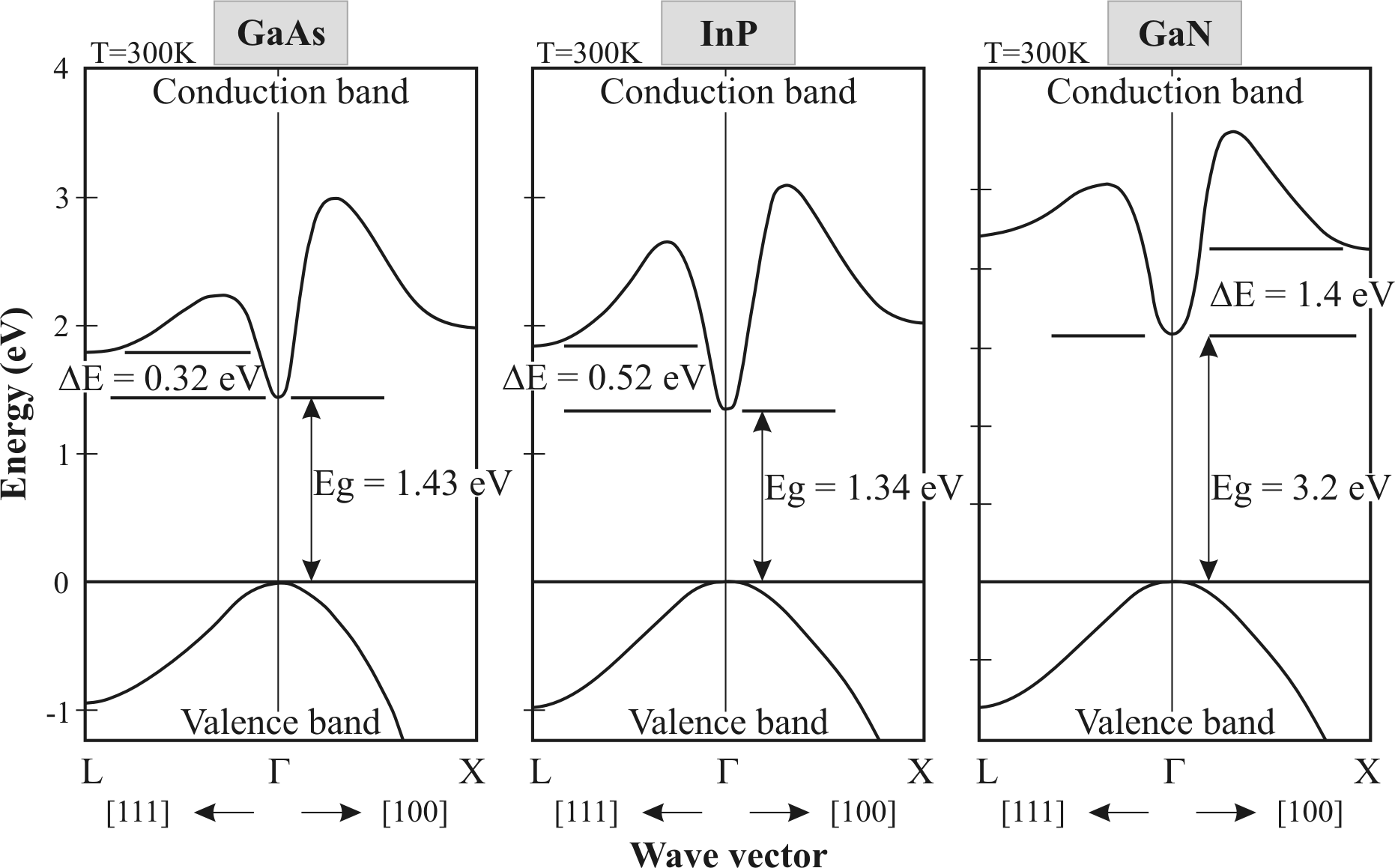
Figure 2.3:
Simplified band structures of zinc-blende (cubic) GaAs, InP and
GaN. [Sze98,Mor99]
|
|
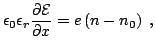
The transferred-electron effect arises from the particular form of
the band structure of some III/V compound semiconductors like
GaAs, InP and GaN. As shown in Fig. 2.3,
these materials are direct band-gap semiconductors, having the
conduction band main minimum in the -point. Two other
satellite valleys2.1 L and
X are in the directions [111] and [100], respectively.
At low
electric fields, the conduction band electrons occupy the bottom
of the central valley. Applying an electric field, the electrons
accelerate until they collide with imperfections of the crystal
lattice. Via collisions, the electrons loose a component of their
momentum, which is directed along the electric field, and some
kinetic energy which raises the lattice temperature (Joule
heating). As the electric field is incremented further, the mean
electron energy becomes higher, and higher energy states can be
occupied in the conduction band. When the electron kinetic energy
reaches the intervalley transfer energy
 (for GaAs
 ), electrons have the additional
choice of occupying one of the satellite valleys (for GaAs the
L-valley), as long as a suitable momentum transfer is also
involved. The electron effective mass
), electrons have the additional
choice of occupying one of the satellite valleys (for GaAs the
L-valley), as long as a suitable momentum transfer is also
involved. The electron effective mass  is depending on the
curvature of the band structure E(k) [IL03]:
is depending on the
curvature of the band structure E(k) [IL03]:
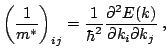 |
(2.1) |
where  is effective mass tensor,
  is the Plank
constant and k is the wave vector. Assuming that the effective
mass tensor components (in the direction of the principal axes)
are equal to , equation 2.1 can be
simplified as:
is the Plank
constant and k is the wave vector. Assuming that the effective
mass tensor components (in the direction of the principal axes)
are equal to , equation 2.1 can be
simplified as:
 |
(2.2) |
In the satellite valleys, the curvature is higher and the
effective mass of the electrons is up to 6 times the
-valley effective mass2.2.
Electrons with sufficient energy have the choice of occupying
either valley. For these electrons there is a higher probability
of occupying the satellite valleys which provide a relatively
high density of states. In the satellite valleys, the electrons
not only posses a higher effective mass, but also undergo strong
scattering processes [BHT72]. The combination of these two
effects explains why the mobility in the side valley  is
up to 70 times lower compared to that in the central valley
is
up to 70 times lower compared to that in the central valley
 . If
. If
 and
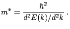
and  are the electron
density in the central and satellite valleys, respectively, the
mean drift velocity
are the electron
density in the central and satellite valleys, respectively, the
mean drift velocity
 is:
is:
 |
(2.3) |
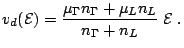
For higher electric fields, more electrons have the sufficient
energy and the satellite valley occupation will increase.
Although an increasing electric field should lead to a higher
electron drift velocity in each valley, the intervalley electron
transfer can compensate this effect and result in a negative
differential mobility. Defining  as the relative L-valley
occupation
as the relative L-valley
occupation
 |
(2.4) |
and assuming that the mobility does not depend on the electric
field, Eq. (2.3) leads to:
 |
(2.5) |
In order to have a negative differential mobility, the following
condition has to be fulfilled:
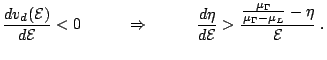 |
(2.6) |
Taking into account that
 is higher than 1 and
lower than 1,
is higher than 1 and
lower than 1,
 must always be
positive, which means that the L-valley relative occupation
() has to increase with the electric field. Equation
2.6 confirms that the intervalley
electron transfer can cause a negative differential mobility.
must always be
positive, which means that the L-valley relative occupation
() has to increase with the electric field. Equation
2.6 confirms that the intervalley
electron transfer can cause a negative differential mobility.
Figure 2.4:
Schematic view of the average electron drift velocity  at 300K as a function of the electric field E for GaAs, InP and GaN [IL03,AWR+98].
|
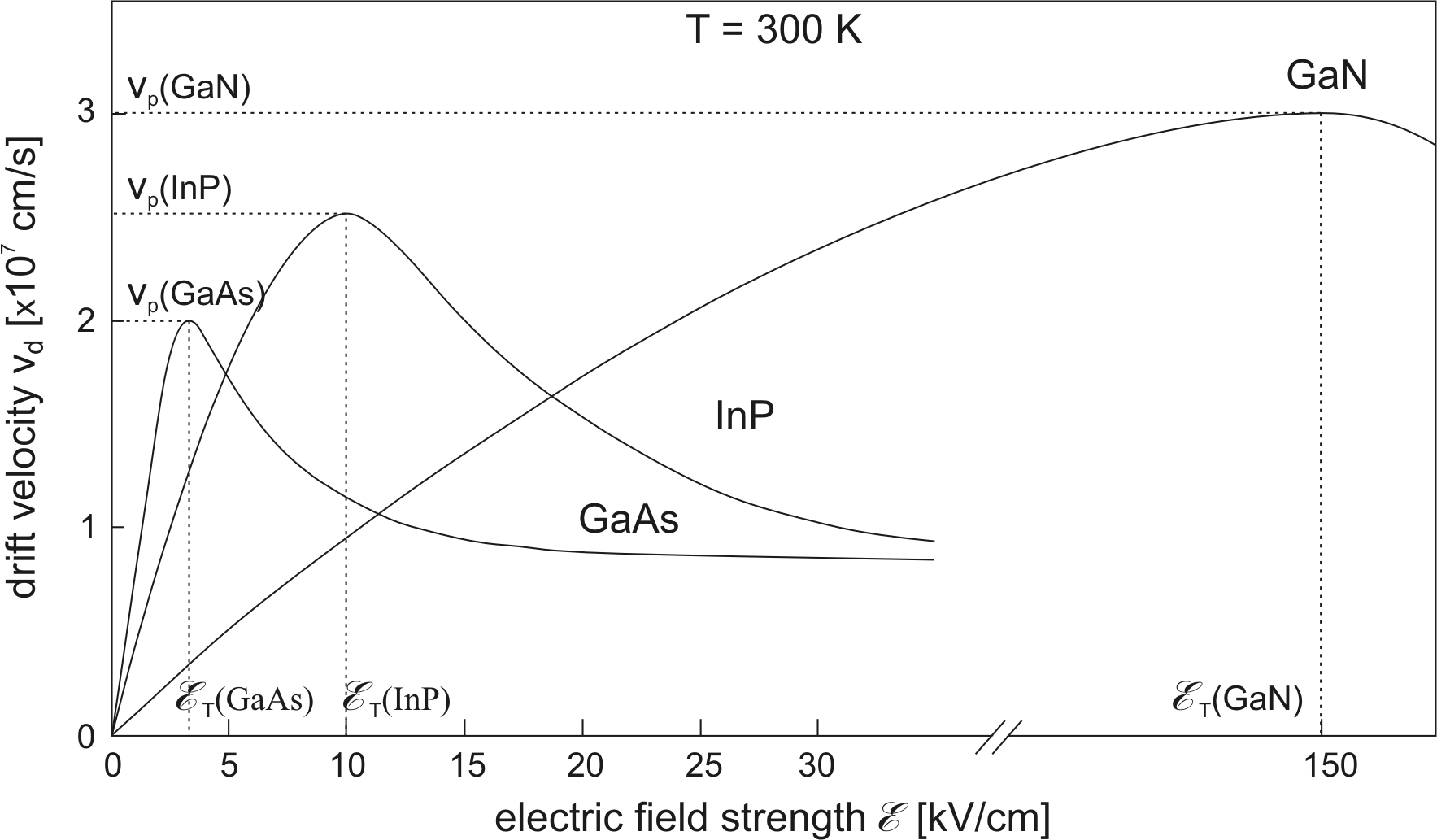
|
Figure 2.4 shows the average electron drift
velocity as a function of the electric field for GaAs, InP and
GaN. The drift velocity raises with the electric field up to the
threshold field
 , hence a negative differential
mobility appears and the drift velocity starts to decrease.
is extremely dependant of the material: in GaAs
is about
, hence a negative differential
mobility appears and the drift velocity starts to decrease.
is extremely dependant of the material: in GaAs
is about
 ,
in InP it is
,
in InP it is
 and in GaN
values between
and in GaN
values between
 and
and
 are reported [KOB+95,AWR+98]
A frequency independent
 characteristics can be
used to describe electron transport in the presence of a
time-varying electric field as long as the frequency of operation
is significantly lower than the relaxation frequency
characteristics can be
used to describe electron transport in the presence of a
time-varying electric field as long as the frequency of operation
is significantly lower than the relaxation frequency  defined
as [AP00]:
defined
as [AP00]:
 |
(2.7) |
where  is the energy relaxation time and
  is
the intervalley relaxation time. For GaAs and GaN, is
1.5 and
is
the intervalley relaxation time. For GaAs and GaN, is
1.5 and
 , respectively and is
7.7 and
, respectively and is
7.7 and
 [BHT72,KOB+95]. Based on these
values, the relaxation frequency of GaAs is found to be
[BHT72,KOB+95]. Based on these
values, the relaxation frequency of GaAs is found to be
 . The frequency capability of GaN is superior, as
indicated by the of
. The frequency capability of GaN is superior, as
indicated by the of
 .
.
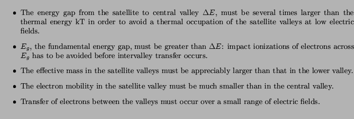
In summary, the material requirements for
transferred-electron
negative differential mobility are [Hob74]:
The negative differential mobility seen in Fig. 2.4
can be exploited directly for AC power generation, if the Gunn
diode is connected to an adequate circuit. Stringent conditions
are placed on its realization and further description will be
given in section 2.3.3 (Low Space-charge
Accumulation, LSA operating mode). One difficulty encountered
when utilizing directly Gunn diodes as AC negative differential
resistances, arises from internal instabilities.
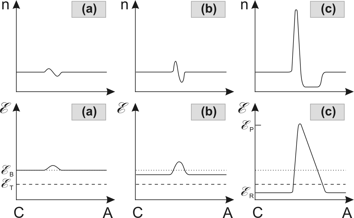
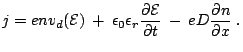
Figure 2.5:
Schematic view of the growth of space-charge fluctuations to a stable dipole domain [Hob74]. C identifies the cathode (emitter) and A the anode (collector).
|
|
To explain how a high-field-domain builds up in a semiconductor
with a negative differential mobility, a simplified example from
Hobson [Hob74] is presented. Let us consider an
uniformly-doped device with an electron concentration  . A
noise process or a defect in the doping uniformity causes a
fluctuation in the electron density
. A
noise process or a defect in the doping uniformity causes a
fluctuation in the electron density  . The fluctuation is an
electric dipole, consisting of a depletion region and an
accumulation region (Fig. 2.5(a)). The
electric field relation to the non-uniformity in the space charge
is given by the Poisson equation:
. The fluctuation is an
electric dipole, consisting of a depletion region and an
accumulation region (Fig. 2.5(a)). The
electric field relation to the non-uniformity in the space charge
is given by the Poisson equation:
 |
(2.8) |
where
 is the relative permittivity and
 is the vacuum permittivity.
If the mean electric field is below the threshold field
, electrons with a higher electric field move
faster than electrons elsewhere. The space charge accumulation
fills in the depletion region and the fluctuation is damped by
dielectric relaxation.
If the mean electric field is above
, the drift
velocity of the electrons in the region of higher field is
reduced. The space-charge region swells
(Fig. 2.5(b)) and, as a consequence of
equation 2.8, the electric field raises in
the region of the domain. In the rest of the device, the electric
field sinks because the total voltage drop must remain constant.
In figure 2.5(c), the domain has
reached a stable condition. The level of the electric field
outside the domain
 is under the threshold and the
electric field in the domain reaches
is under the threshold and the
electric field in the domain reaches
 .
and
correspond to the same drift
velocity. Inside the domain, electrons travel as fast as outside
the domain and the space-charge region stops growing. When a
domain is stable, no other domain can build up while
is below the threshold.
.
and
correspond to the same drift
velocity. Inside the domain, electrons travel as fast as outside
the domain and the space-charge region stops growing. When a
domain is stable, no other domain can build up while
is below the threshold.
2.1.3 Domain Dynamics
In this section, the behaviour of stable domains will be examined.
The stable space charge profile, or domain, drifts at a constant
velocity through the device. The electric field in the different
parts of this nonlinear entity is strictly related to the domain
growth and decay and to the corresponding stability. The analysis
of the domain form requires non linear solutions of the Poisson
equation and the current continuity equation taking the
characteristics into account. An analytical
solution of the problem comes from Butcher et al. [But65,BFH66]. Their most important results can be summarized in three
items:
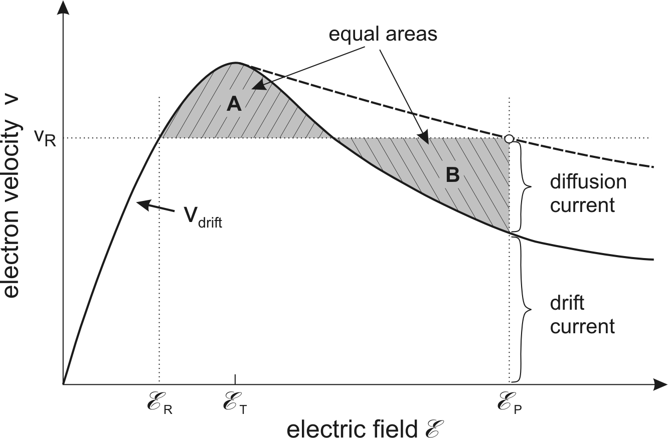
The conserved2.3 current density  is given by:
 |
(2.10) |
where the three terms represent, respectively, the drift,
displacement and diffusion component. Equation
(2.10) is simplified outside the
domain, where and
 are independent of the
position. The current is carried entirely as drift current. Inside
the domain, all three terms of Eq. (2.10) play
a role. The electric field gradients move and determine the
displacement current to flow. At the peak field of the domain,
there is no displacement current because
are independent of the
position. The current is carried entirely as drift current. Inside
the domain, all three terms of Eq. (2.10) play
a role. The electric field gradients move and determine the
displacement current to flow. At the peak field of the domain,
there is no displacement current because
 , but the electron density gradient results in a diffusion
current. Figure 2.6 illustrates the
relative values between diffusion and drift currents. For the
depletion region of the domain, the current is predominantly
carried by a displacement current, while in the accumulation
region there is a large drift current opposed by displacement and
diffusion currents.
, but the electron density gradient results in a diffusion
current. Figure 2.6 illustrates the
relative values between diffusion and drift currents. For the
depletion region of the domain, the current is predominantly
carried by a displacement current, while in the accumulation
region there is a large drift current opposed by displacement and
diffusion currents.
Figure 2.7:
Domain profile in the limit condition of zero
diffusion.
| 7cm
|
Further on, the form of a stable high field domain will be
examined, neglecting the diffusion and it will be shown that the
domains travel at the same velocity (
 ) as the
electrons outside the domain(
) as the
electrons outside the domain( ). If the diffusion coefficient
D is assumed to be zero, the electron density of the domain must
be zero (depletion region) or
). If the diffusion coefficient
D is assumed to be zero, the electron density of the domain must
be zero (depletion region) or  (accumulation region)
[Hob74]. In this simple case, the electric field in the
domain is triangular, as shown in Fig. 2.7.
Outside the domain, nothing changes and the carrier concentration
remains . The current density outside the domain is
(accumulation region)
[Hob74]. In this simple case, the electric field in the
domain is triangular, as shown in Fig. 2.7.
Outside the domain, nothing changes and the carrier concentration
remains . The current density outside the domain is
 |
(2.11) |
Inside the domain, in the case of a fully depleted region, the
current density is written:
 |
(2.12) |
The Poisson equation requires:
 |
(2.13) |
therefore
 |
(2.14) |
By current continuity ( ), Eq. (2.11) and
Eq. (2.14) require that
), Eq. (2.11) and
Eq. (2.14) require that
 |
(2.15) |
In the case of a fully depleted domain, the result is not
influenced by the electric field dependence of the diffusion
constant D.
The next problem consists in finding the stable value of the
outside field
in connection with the applied
terminal bias  . If
. If  is the device length,
  the width
of the domain and
the width
of the domain and  the domain voltage, is given by:
 |
(2.16) |
The domain length can be neglected, because it is small in
comparison with the device length ( ), therefore:
 |
(2.17) |
, in the case of the triangular domain (with the diffusion
coefficient D=0) is given by:
 |
(2.18) |
From the Poisson equation
 |
(2.19) |
resulting for the expression:
 |
(2.20) |
Equation (2.20), the electrical boundary
condition (Eq. (2.17)) and the equal area
rule between
 and
determine the
domain behaviour for a given terminal bias .
and
determine the
domain behaviour for a given terminal bias .
Figure 2.8 outlines the
relationship between the domain voltage and the electric field
outside the domain. In the diagram, the three load lines
correspond to three different terminal biases . The
intercepts are the possible solutions for a given doping
concentration  , device length . The electrical field
is displayed versus the domain voltage .
Three configurations are possible:
, device length . The electrical field
is displayed versus the domain voltage .
Three configurations are possible:
- Load line 1.
- The
average electric field
 (the intersection of the load-line
with the
-axis) is higher than threshold field
.
Under this condition, only one solution is possible and the
solution is stable.
(the intersection of the load-line
with the
-axis) is higher than threshold field
.
Under this condition, only one solution is possible and the
solution is stable.
- Load line 2.
- The
average electric field is equal to
 . The value
  is called
sustaining voltage. Under this characteristic voltage the
domain will be extinguished in flight. At the sustaining voltage, the
load-line is tangent to the
is called
sustaining voltage. Under this characteristic voltage the
domain will be extinguished in flight. At the sustaining voltage, the
load-line is tangent to the
 curve. is
extremely important concerning the analysis of the oscillation
modes.
curve. is
extremely important concerning the analysis of the oscillation
modes.
- Load line 3.
- The
average electric field is lower than
 and
higher than
. If
the value has been higher than
during the domain
nucleation, two solutions are possible. The higher intercept is stable, the
lower one unstable.
and
higher than
. If
the value has been higher than
during the domain
nucleation, two solutions are possible. The higher intercept is stable, the
lower one unstable.
Keeping in mind that the load line condition
(Eq. (2.17)) must be satisfied all the time
and that the
curve refers only to a steady state domain,
the instability of the lower intercept can be explained with a simple example.
Let us consider a small noise fluctuation: a small increase of
causes
to decrease (Eq. (2.17)).
The new state is not anymore on the
curve, but higher. In the
new state, the electrons outside the domains move faster than
the domain. This means that both the accumulation and depletion
regions of the domain will grow causing a further increase of
(Poisson's equation). In the next state, the working
point will move again higher on the load-line and the readjustment will
continue up to the higher stable intercept.
2.1.4 The small signal behaviour of a transferred-electron
device
In this section, the
stability with respect to small current or voltage perturbations
of the steady-state solutions will be considered [MC66,Hei71]. The analysis starts from the Poisson's and current
equations:
and from two assumptions about the fluctuations:
- the fluctuations are periodic in time;
- the fluctuations are small in comparison to the
corresponding equilibrium values
 ,
,  and
and  .
.
The so defined fluctuations are governed by:
From Eq. (2.21) and Eq. (2.23) it
follows:
 |
(2.26) |
and
 |
(2.27) |
Equations (2.23),
(2.24) and (2.25) can
be substituted in the current equation
(2.22) and can be eliminated with the
help of Eq. (2.27), obtaining:
 |
(2.28) |
After some simplifications:
 |
(2.29) |
The last term in Eq. (2.29) can be
neglected, because it is of the same order as 
 ) and
) and
 was assumed to be small.
 |
(2.30) |
If the doping concentration in the active region is uniform,
is not depending on  and Eq. (2.30)
results in a linear differential equation with constant
coefficients. Choosing
and Eq. (2.30)
results in a linear differential equation with constant
coefficients. Choosing
 as boundary
condition, the general solution is:
as boundary
condition, the general solution is:
 |
(2.31) |
where
 |
(2.32) |
Finally, from Eq. (2.23) and
Eq. (2.31), we have:
 |
(2.33) |
The second term on the right side of
Eq. (2.33) describes an uniform field
oscillation, independent of ; this governs in the LSA operating
mode (see section 2.3.3). The last term
represents a wave propagating in the direction with the same
phase and group velocity , because using
(2.32) we obtain:
![$\displaystyle v_{phase}\equiv \frac{\omega}{Im[\gamma]}=v_0 \thickspace ,\thic...
...v_{group}\equiv \frac{\partial \omega}{\partial(Im[\gamma])}=v_0 \thickspace .$](http://web.tiscali.it/decartes/phd_html/img133.png) |
(2.34) |
This variable was defined as the drift velocity, at
which the electrons move through the crystal under the influence
of the external electrical field. The modulation
 of the electron density
creates a space charge wave, which propagates with the
electron drift velocity .
of the electron density
creates a space charge wave, which propagates with the
electron drift velocity .
If  , then
![$ Re[\gamma] > 0$](http://web.tiscali.it/decartes/phd_html/img136.png) and the wave is damped; if
and the wave is damped; if
 , then
![$ Re[\gamma] < 0$](http://web.tiscali.it/decartes/phd_html/img138.png) and the wave amplitude increases.
The sign of
and the wave amplitude increases.
The sign of  depends first of all on the electric field in
relation to the threshold field
, as already
explained in section 2.1.2 and
shown in
Fig. 2.4.
depends first of all on the electric field in
relation to the threshold field
, as already
explained in section 2.1.2 and
shown in
Fig. 2.4.
The device is stable with respect to small perturbations if the
real part of the impedance  is positive. is defined as:
 |
(2.35) |
where  is the cross sectional area of the Gunn device. With
Eq. (2.31) it follows:
is the cross sectional area of the Gunn device. With
Eq. (2.31) it follows:
 |
(2.36) |
As demonstrated by McCumber and Chynoweth [MC66],
Eq. (2.36) is well behaved for all finite
 and
and  has no singularities. This means that the
device described by Eq. (2.36) is always stable
when it operates under constant current conditions.
has no singularities. This means that the
device described by Eq. (2.36) is always stable
when it operates under constant current conditions.
In order to determine the stability under constant
voltage conditions, the poles of the admittance
 or the zeros of must be
investigated. Setting
or the zeros of must be
investigated. Setting
 , the zeros of
Eq. (2.36) correspond to the zeros
, the zeros of
Eq. (2.36) correspond to the zeros
 (n=0,1,2..) of
 |
(2.37) |
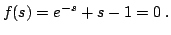
It is necessary to divide f(s) into the real and imaginary part:
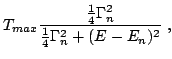
- The first zero is
 : this means
 . Either the length of the device is zero (L=0) or the
frequency and the mobilities are zero (
. Either the length of the device is zero (L=0) or the
frequency and the mobilities are zero ( ).
).
is not a physically relevant zero of .
- The other zeros
 (n=1,2,3..) satisfy the
conditions:
(n=1,2,3..) satisfy the
conditions:
 |
 |
![$\displaystyle \frac{(4n+1)\pi}{2}-\arcsin\left[(1-\phi_n)e^{\phi_n}\right]\thickspace,$](http://web.tiscali.it/decartes/phd_html/img161.png) |
(2.41) |
 |
|
![$\displaystyle -\frac{1}{2}\thickspace \ln\left[\eta_n^2+(1-\phi_n^2)\right]\thickspace,$](http://web.tiscali.it/decartes/phd_html/img163.png) |
(2.42) |
 |
|
 |
(2.43) |
 |
|
![$\displaystyle -ln\left[\frac{(4n+1)\pi}{2}\right]\thickspace .$](http://web.tiscali.it/decartes/phd_html/img167.png) |
(2.44) |
The second zero is for
 .
.
If
 , then the Re[Z] is positive and the device is
stable. From Eq. (2.32), it results:
, then the Re[Z] is positive and the device is
stable. From Eq. (2.32), it results:
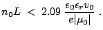 |
(2.45) |
Choosing the parameters for GaAs (
 ,
,
 and
and
 ),
we have:
),
we have:
 |
(2.46) |
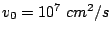
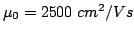
Considering that the mobility depends on the doping level, the
consistent stability condition for GaAs is given by:
 |
(2.47) |
It can be concluded that, at room temperature, GaAs devices will
always be stable with steady state properties, if the product
 is under the critical value. This result applies only for a
small signal approach; nevertheless, with appropriate intensity of
the electric field (i.e.
is under the critical value. This result applies only for a
small signal approach; nevertheless, with appropriate intensity of
the electric field (i.e.
 ), samples with
lower than the critical value provide amplification for
microwave signals (i.e.
).
), samples with
lower than the critical value provide amplification for
microwave signals (i.e.
).
2.2 Gunn diode with hot electron injectors
Hot electron injection is the process of raising the electron
energy to the level of the L band before it enters the drift zone.
Without a hot electron injector, the electrons will remain in the
-valley until they gain enough energy to transfer to the
upper valleys. The distance required to gain such an energy
depends on the electric field level and, on a minor scale, on the
device temperature. The region near the emitter, where most
electrons reside in the -valley, is called
dead-zone. Gunn domains can build only outside the
dead-zone. The dead-zone not only narrows the active region (up to
17% in a
 GaAs Gunn device [NDS+89]),
but introduces an undesirable positive serial resistance reducing
the r.f. power and the efficiency of the device. Moreover, the
dead zone is not constant and should be considered as an aleatory
process having very bad influences on the device noise properties.
GaAs Gunn device [NDS+89]),
but introduces an undesirable positive serial resistance reducing
the r.f. power and the efficiency of the device. Moreover, the
dead zone is not constant and should be considered as an aleatory
process having very bad influences on the device noise properties.
The solution to the described problems is to embed a hot electron
injector in the emitter region just before the Gunn diode active
region. An efficient injector leads to the following advantages:
- improved temperature stability of power and frequency,
- improved oscillator turn on
characteristic, especially at low temperatures,
- increased efficiency (lower voltage drop on
the injector),
- low phase noise.
The Schottky, graded gap and resonant tunneling injectors
represent different approaches to fulfill these objectives.
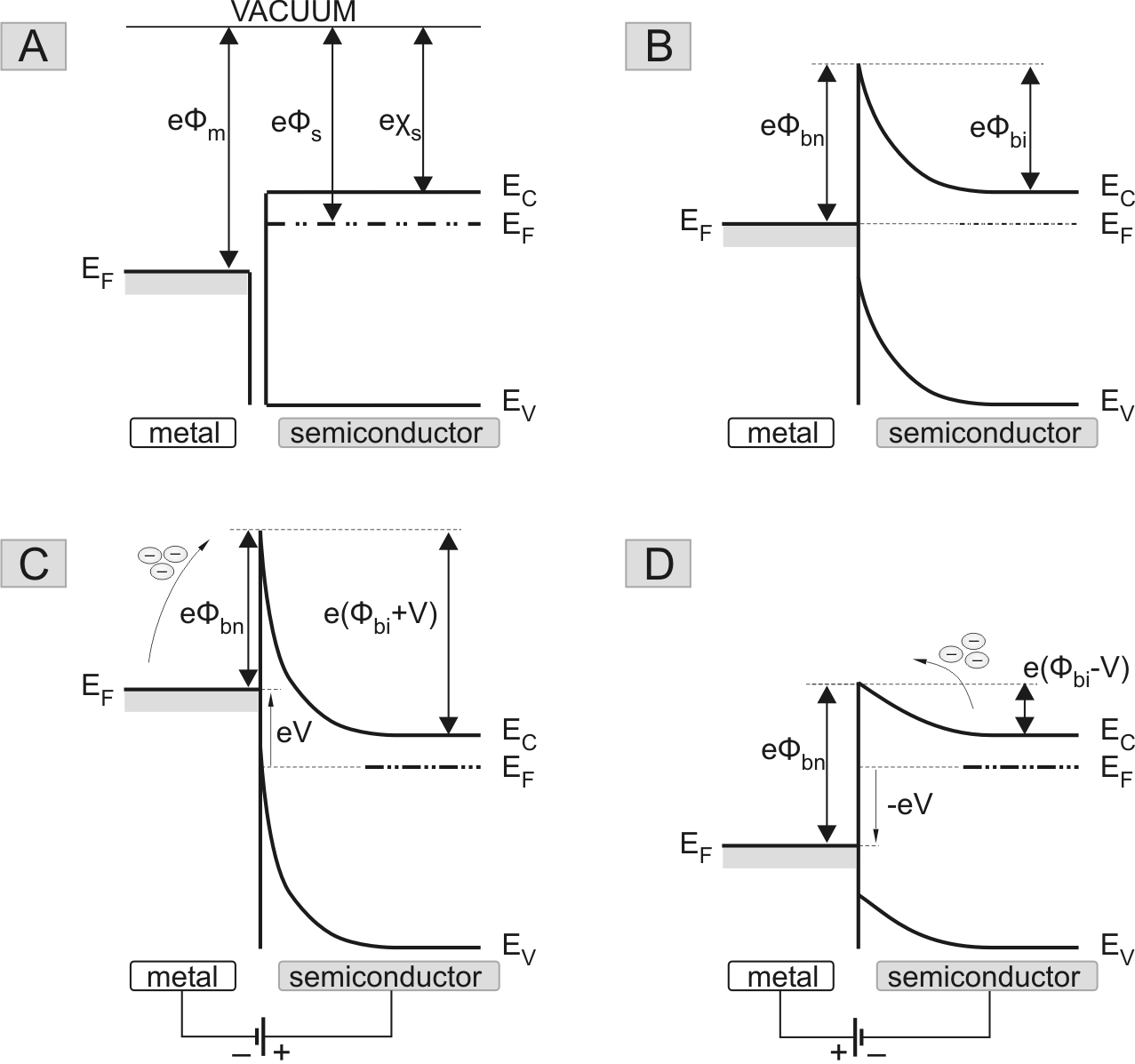
2.2.1 Metal semiconductor Schottky contact injector
To understand how the Schottky contact injector works, it is
useful to introduce briefly the physics behind a
metal-semiconductor contact.
Figure 2.9:
Energy-band diagrams for Schottky contact on n-semiconductor: (a) before contacting,
(b) after contacting in equilibrium, (c) under reverse bias and (d) direct bias.
|
|
There are two kinds of metal-semiconductor contacts: ohmic and
Schottky. An ohmic contact is a metal or silicide contact to a
semiconductor with a small interfacial resistance and a linear I-V
characteristics. In this case, the work function of the
semiconductor must be greater than the work function of the metal
(
 ) [Nea97]. The described condition is
valid only for ideal ohmic contacts (e.g. indium based
compounds). Typically, semiconductor engineers consider ohmic
contacts also Schottky contacts with a very thin
potential barrier and a linear I-V characteristic.
) [Nea97]. The described condition is
valid only for ideal ohmic contacts (e.g. indium based
compounds). Typically, semiconductor engineers consider ohmic
contacts also Schottky contacts with a very thin
potential barrier and a linear I-V characteristic.
In a Schottky contact, the work function of the semiconductor must
be smaller than the work function of the metal (
 ). The ideal energy-band diagram for a particular metal
and n-type semiconductor before making the contact is shown in
Fig. 2.9(a), where
). The ideal energy-band diagram for a particular metal
and n-type semiconductor before making the contact is shown in
Fig. 2.9(a), where
 is the metal work function,
 is the semiconductor work function and
 is the semiconductor electron affinity. The vacuum
level is used as a reference level. Before contacting, the Fermi
level in the metal is above the Fermi level in the semiconductor.
After contacting, in thermal equilibrium, the Fermi level has to
be constant through the whole system and electrons from the
semiconductor flow into the lower energy states in the metal.
Positively charged donor atoms remain in the semiconductor,
creating a space charge region (Fig.
2.9(b)). The potential barrier seen
by electrons in the metal trying to move into the semiconductor is
known as ``Schottky barrier''. Assuming an ideal interface,
without Fermi pinning, the barrier height
is the semiconductor electron affinity. The vacuum
level is used as a reference level. Before contacting, the Fermi
level in the metal is above the Fermi level in the semiconductor.
After contacting, in thermal equilibrium, the Fermi level has to
be constant through the whole system and electrons from the
semiconductor flow into the lower energy states in the metal.
Positively charged donor atoms remain in the semiconductor,
creating a space charge region (Fig.
2.9(b)). The potential barrier seen
by electrons in the metal trying to move into the semiconductor is
known as ``Schottky barrier''. Assuming an ideal interface,
without Fermi pinning, the barrier height
 is
given by:
is
given by:
 |
(2.48) |
On the semiconductor side,
 is the built-in
potential barrier seen by electrons in the conduction band trying
to move into the metal and is given by:
is the built-in
potential barrier seen by electrons in the conduction band trying
to move into the metal and is given by:
 |
(2.49) |
where  is the potential difference between the minimum
of the conduction band in the semiconductor (
is the potential difference between the minimum
of the conduction band in the semiconductor (
 ) and
the Fermi level (
) and
the Fermi level (
 ):
):
 |
(2.50) |
where  is the electron charge.
In the reverse bias condition, where a positive voltage
 is applied to the semiconductor with respect to the
metal (Fig. 2.9(c)), the
semiconductor-to-metal barrier increases, while
remains constant in the idealized case. In
the forward bias condition, a negative voltage is applied to the
semiconductor with respect to the metal (Fig.
2.9(d)) and the
semiconductor-to-metal barrier decreases, while
still remains constant. In this case,
electrons can move easily from the semiconductor into the metal.
is applied to the semiconductor with respect to the
metal (Fig. 2.9(c)), the
semiconductor-to-metal barrier increases, while
remains constant in the idealized case. In
the forward bias condition, a negative voltage is applied to the
semiconductor with respect to the metal (Fig.
2.9(d)) and the
semiconductor-to-metal barrier decreases, while
still remains constant. In this case,
electrons can move easily from the semiconductor into the metal.
Solving the Poisson's equation, it is possible to
calculate the electric field present in the space charge region in
the metal. The depletion layer width  of region is given by:
 |
(2.51) |
where  is the donor concentration,
 is the
dielectric constant of the semiconductor, k is the Boltzmann
constant and T is the temperature in K. The term kT/e arises from
the contribution of the majority-carrier distribution tail
[Sze81].
is the
dielectric constant of the semiconductor, k is the Boltzmann
constant and T is the temperature in K. The term kT/e arises from
the contribution of the majority-carrier distribution tail
[Sze81].
Three basic transport processes through the Schottky
barrier can be identified:
- thermionic emission of electrons over the potential
barrier (dominant process for moderate doped semiconductor
 ),
),
- tunneling of electrons through the barrier
(quantum-mechanical process important for heavily doped semiconductors and responsible for most ohmic
contacts),
- recombination in the depletion region.
The ideal expression of the J-V characteristics taking
into account the thermionic emission and the diffusion is
[Sze81]:
 |
(2.52) |
The saturation current density,  for the
thermionic emission case is:
for the
thermionic emission case is:
 |
(2.53) |
where  is the effective Richardson constant. Tunneling,
recombination and injection cause deviations from the ideal
behaviour. Introducing the serial resistance2.4
is the effective Richardson constant. Tunneling,
recombination and injection cause deviations from the ideal
behaviour. Introducing the serial resistance2.4  and the ideality
factor leads to
and the ideality
factor leads to
 |
(2.54) |
Looking back at the first Gunn diodes, a Schottky barrier was
always present. The quality of the ohmic contacts was extremely
poor, leading to low uniformity, low reproducibility and high
parasitic voltage drops.
Even if, in the last 30 years, amazing
improvements have been achieved in metal-semiconductor contacts,
an unsolvable problem remains for Schottky hot electron injectors:
Fermi level pinning. The Schottky barrier on GaAs has a height of
about
 , not depending of the metal because of
the Fermi level pinning. The barrier cannot be engineered properly
and
is not the optimum barrier height for an
efficient electron transfer from to L valley. In a
similar way, Fermi level pinning is present also in other III/V
semiconductors, limiting the applications of the Schottky barrier
injector Gunn diodes drastically.
, not depending of the metal because of
the Fermi level pinning. The barrier cannot be engineered properly
and
is not the optimum barrier height for an
efficient electron transfer from to L valley. In a
similar way, Fermi level pinning is present also in other III/V
semiconductors, limiting the applications of the Schottky barrier
injector Gunn diodes drastically.
2.2.2 Graded gap injector
The idea of the graded gap AlGaAs barrier comes from the need of a
potential barrier which can be optimized, changing its height,
width and shape [CBK+88,NDS+89,GWCE88]. As seen in section
2.2.1, these parameters are difficult
to control in the case of the metal-semiconductor Schottky
barrier, especially concerning the reproducibility.
Figure 2.10:
Principle schema of a Gunn diode with a graded AlGaAs
injector. C identifies the cathode (emitter) and A the anode
(collector).
| 7.5cm
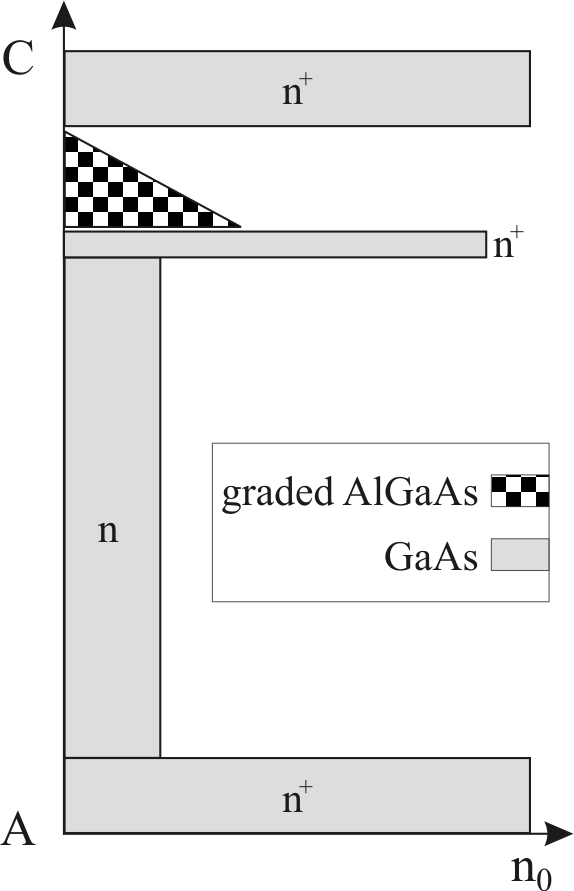
|
The epitaxial process offers an extremely high accuracy and
tuning possibilities for the injector fabrication. The material
system
 maintain nearly the same lattice
constants, with the change of the Al concentration. Grading the
Al concentration, it is possible to obtain a potential barrier.
The AlGaAs barrier has to be nominally undoped and the Al
concentration starts at 0% (on the cathode/emitter side) and
increases linearly up to the maximal concentration (in the
anode/collector direction). The height of the barrier has to be
designed considering the energy
needed by electrons for the to transfer.
maintain nearly the same lattice
constants, with the change of the Al concentration. Grading the
Al concentration, it is possible to obtain a potential barrier.
The AlGaAs barrier has to be nominally undoped and the Al
concentration starts at 0% (on the cathode/emitter side) and
increases linearly up to the maximal concentration (in the
anode/collector direction). The height of the barrier has to be
designed considering the energy
needed by electrons for the to transfer.
Establishing the width of the graded AlGaAs barrier, two factors
have to be considered. The barrier has to be wide enough to
prevent electrons to tunnel at lower energy levels; only the
electrons passing over the barrier have enough energy for the
intervalley transfer. On the other hand, a wide undoped AlGaAs
barrier results in a too high serial resistance. The second part
of the injector is a thin  doped layer of GaAs, connecting
the AlGaAs barrier to the Gunn active region. A complete view of
the graded gap injector is illustrated in
Fig. 2.10.
doped layer of GaAs, connecting
the AlGaAs barrier to the Gunn active region. A complete view of
the graded gap injector is illustrated in
Fig. 2.10.
In order to correctly understand the behaviour of the graded gap
injector Gunn diodes, complex simulations are required. Monte
Carlo computations have demonstrated that the graded AlGaAs
barrier, followed by a thin highly doped layer, increases the
intervalley electron transfer and reduces the dead-zone
thereby improving noise performance, temperature stability and
power conversion efficiency [LR90]. A much simpler approach
for the simulation of the DC behaviour considers the Gunn diode
composed of two elements in series: the graded gap injector and
the diode active region plus the contact resistance. For low bias
(voltages much lower than the threshold), the Gunn active region
plus the contact resistance have a linear characteristics and the
graded gap injector can be modelled like a Schottky barrier. Under
these assumptions, a load-line model is defined like in
Fig. 2.11 where the voltage drop on
the diode  is the sum of the single voltage drops, on the
graded gap injector (
is the sum of the single voltage drops, on the
graded gap injector ( ) and on the ohmic active region
(
) and on the ohmic active region
( ).
).
Figure 2.11:
DC electrical model of a graded gap injector Gunn
diode.
|
|
The following function describes the graded gap injector with a
simple exponential law. Two important parameters are introduced:
the saturation current  (Eq. (2.53)) and
the constant
(Eq. (2.53)) and
the constant  , which is a measure of the tunneling current.
 |
(2.55) |
Then, considering the device area and the active region
length  , the current
  through the active region can be
written as:
through the active region can be
written as:
 |
(2.56) |
The resistivity  can be expressed as:
 |
(2.57) |
where is the electron concentration,  is the mobility and
is the electron charge. Introducing the Lambert transcendental
function W(x) and defining the diode current as
is the mobility and
is the electron charge. Introducing the Lambert transcendental
function W(x) and defining the diode current as
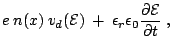
 , it follows:
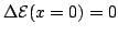
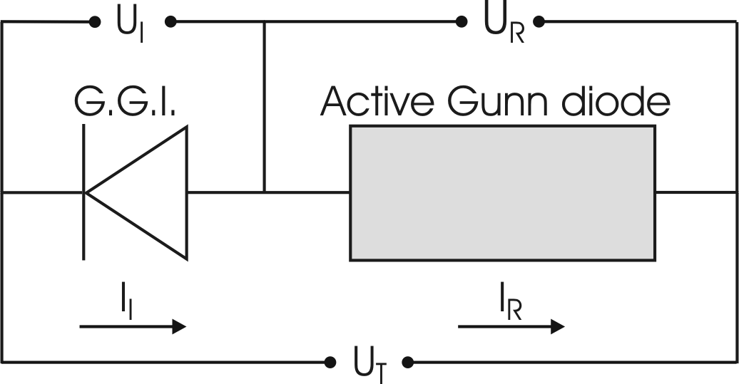
Substituting in Eq. (2.55), the diode current
 is obtained as function of the diode total bias
 |
(2.60) |
As shown in section 6.1.3,
Eq. (2.60) matches the I-V behaviour of
graded gap Gunn diode very well. The proposed model is fitted to
the measured I-V characteristic in the reverse current direction
for different temperatures. Moreover, taking into account the
temperature dependence of , the effective barrier height can
be estimated.
2.2.3 Resonant tunneling injector
In section 2.2.2, the state of the art for
hot electron injection in Gunn diodes has been discussed . This
raises the question if a graded gap injector can be further
improved. The solution might be in using the resonant tunneling
effect, one of the most exciting quantum mechanical phenomena in
semiconductor physics [CET74,TE73].
Figure 2.12:
Bias-dependent band diagrams and current voltage characteristics for an RTD at 4 bias points: A, B,
C, D.
|
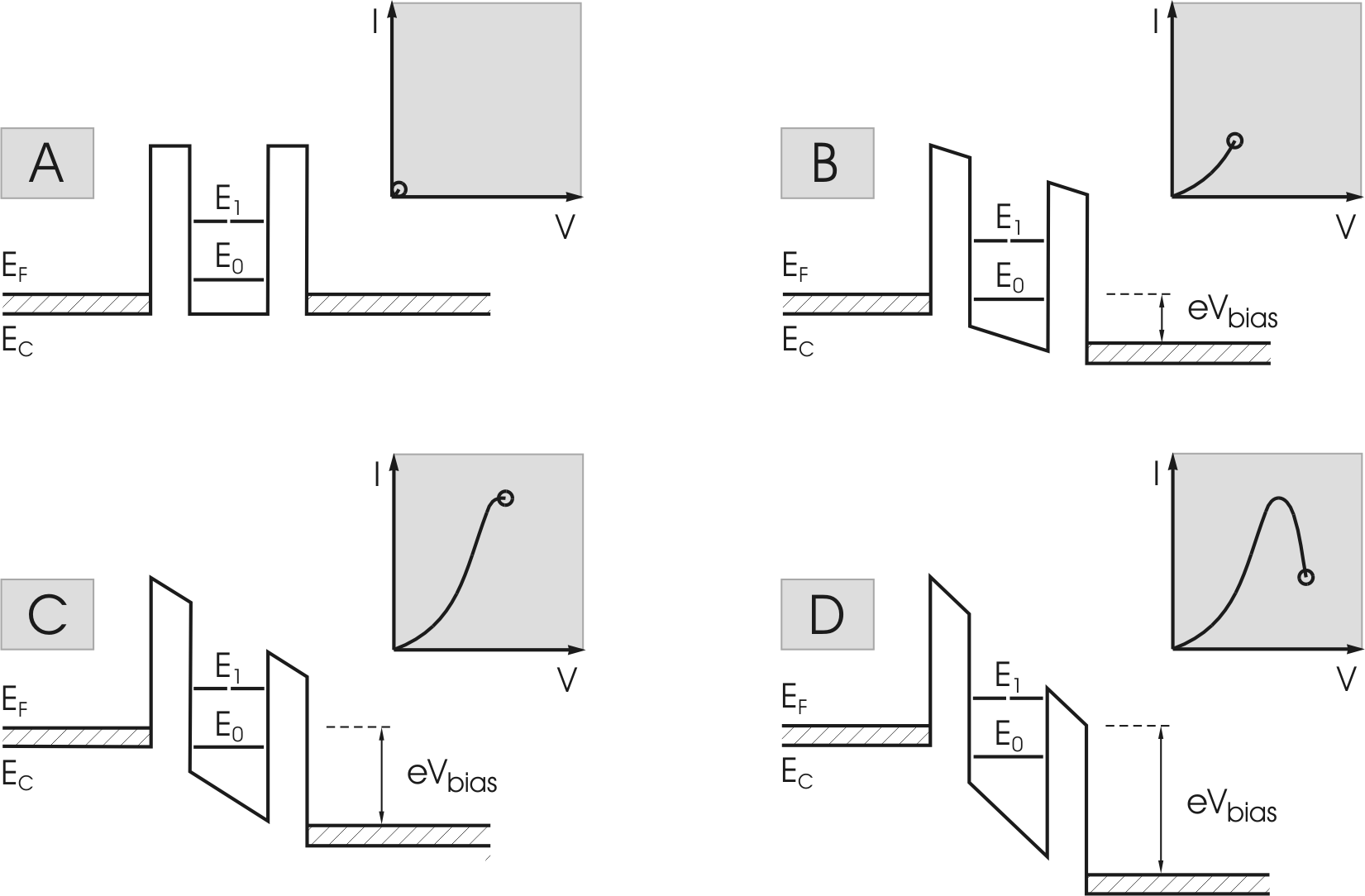
|
Resonant tunneling diodes (RTDs) are based on a double potential
barrier structure like AlAs/GaAs/AlAs. The structure is designed
such that resonant bound states are present in the quantum well.
Electrons can tunnel through the double-barrier if their
transversal energy is equal to the energy of one of the quasi
bound states in the quantum well. The I-V curve of a double
barrier structure can be in principle understood with the help of
Fig. 2.12. Close to zero electrical bias, a small
fraction of the electrons has an energy equal with the energy of
the first quasi bound state (Fig. 2.12A). As the
voltage increases, the resonant states are shifted down towards
the Fermi level on the emitter side and a greater number of
electrons can tunnel, contributing to the current
(Fig. 2.12B). At a certain voltage, the conduction
band level of the emitter side is aligned to the quantum well
resonant level and a maximum
appears in the current (Fig. 2.12C). Beyond this
voltage, the resonant level drops below the emitter conduction
band edge, resulting in a sudden drop of the current
(Fig. 2.12D). For higher voltages, the current rises
again, because of the combination of two effects: the next
resonant level lowers and a thermionic emission occurs over the
barrier.
The negative differential resistance of the RTD
(Fig. 2.12D) has been exploited for microwave analog
devices like oscillators [BPBP93] and mixers [MMP+91] and
for ultrafast digital devices like monostable-bistable transition
logic elements (MOBILE) [MM93,SMI+01,Was03].
Figure 2.13:
Band diagram of a typical GaAs/AlGas heterostructure (A) with the corresponding transmission probability T (B).
The electron distribution before and after the double barrier points out the excellent energy filter capabilities of the device.
|
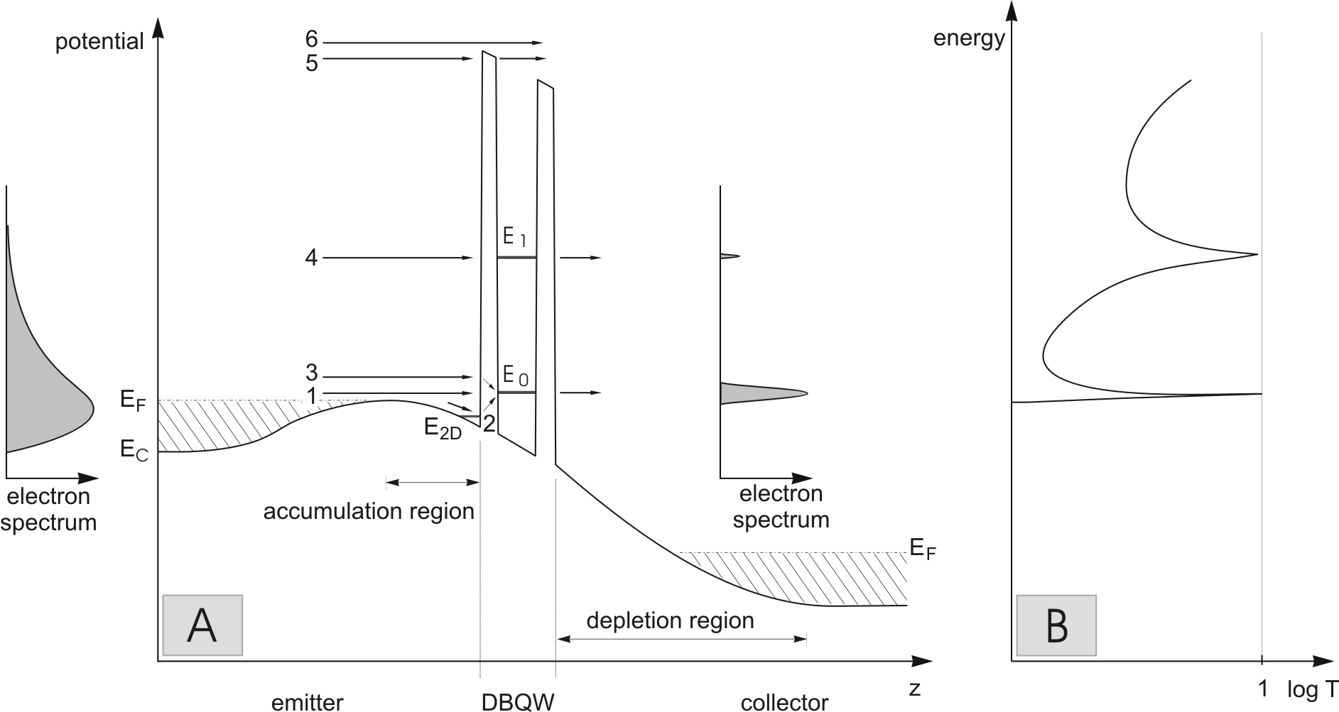
|
For RTD serving as a hot electron injector, no negative
differential resistance is needed and only the small bias voltage
region of the I-V curve should be considered. As a means to better
understand the resonant tunneling injection, the different
transport processes through a double barrier are examined
[SHMS98]. In Fig. 2.13(A), the different
transport paths are illustrated. The electrons with exactly the
resonant energy  tunnel through the double barrier with the
probability of
tunnel through the double barrier with the
probability of  (process 1). In the emitter part, the
electron accumulation in front of the first barrier bends the
conduction band and causes the formation of a triangular potential
well with discrete two-dimensional energy levels. Electrons can
tunnel from the potential well through the double barrier with
the help of a phonon (process 2). In a similar way, electrons
undergoing the process 3, whose energy is a little higher than the
resonant energy , can tunnel due to an interaction with a
phonon. In process 4, like in process 1, electrons have exactly
the energy of the resonant level
(process 1). In the emitter part, the
electron accumulation in front of the first barrier bends the
conduction band and causes the formation of a triangular potential
well with discrete two-dimensional energy levels. Electrons can
tunnel from the potential well through the double barrier with
the help of a phonon (process 2). In a similar way, electrons
undergoing the process 3, whose energy is a little higher than the
resonant energy , can tunnel due to an interaction with a
phonon. In process 4, like in process 1, electrons have exactly
the energy of the resonant level  . In process 5-6, high
energy electrons cross the device, tunneling through only one
barrier or overcoming the whole heterostructure (thermionic
emission). Because of the required high energy, electrons involved
in process 5 and 6 are relatively few.
. In process 5-6, high
energy electrons cross the device, tunneling through only one
barrier or overcoming the whole heterostructure (thermionic
emission). Because of the required high energy, electrons involved
in process 5 and 6 are relatively few.
The electron transmission probability T is a result of the
different transport processes. In a first approximation, T can be
expressed as a Lorentzian function of energy E with a half width
 [Dav98]:
where  and
and  represent the transmission probability of
the single barriers, the full energetic width at half
maximum of the transmission probability T and
represent the transmission probability of
the single barriers, the full energetic width at half
maximum of the transmission probability T and  is the
electron lifetime in the energy state
is the
electron lifetime in the energy state  .
.
The simulated T versus the electron energy is plotted in
Fig. 2.13(B). It can be noticed a tunneling
probability of one for the quantized energy states. The width of
the resonance is exponentially dependent on the thickness of the
barrier. Direct effects of the resonance can be seen in the
electron distribution behind the double barrier. This confirms
that this device can be used for building a very precise energy
filter.
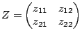
2.3.1 Theory of two-port networks
All electromagnetic processes can ultimately be explained by
Maxwell's four basic equations:
 |
|
 |
(2.64) |
 |
|
 |
(2.65) |
 |
|
 |
(2.66) |
 |
|
 |
(2.67) |
However, it is not always possible or convenient to
directly use these equations. Solving them can be quite difficult.
Efficient design requires the use of approximations such as lumped
and distributed models.
Linear or nonlinear networks, operating with signals small enough
for the networks to respond in a linear manner, can be completely
characterized by parameters measured at the network terminals
(ports), no matter of the network contents. Once the parameters of
a network are determined, its behaviour in any external
environment can be predicted, again without regard to the network
contents. Although a network may have any number of ports, network
parameters can be explained most easily by considering a network
with only two ports, an input port and an output port, like in
Fig. 2.14. To characterize a network, any of the
several parameter sets can be chosen; each of these offers certain
advantages [Pac96]. Each parameter set is related to a group of
four variables associated with the two-port model. Two variables
represent the excitation of the network (independent variables),
and the other two represent the response of the network to the
excitation (dependent variables).
Figure 2.14:
General two-port network
|
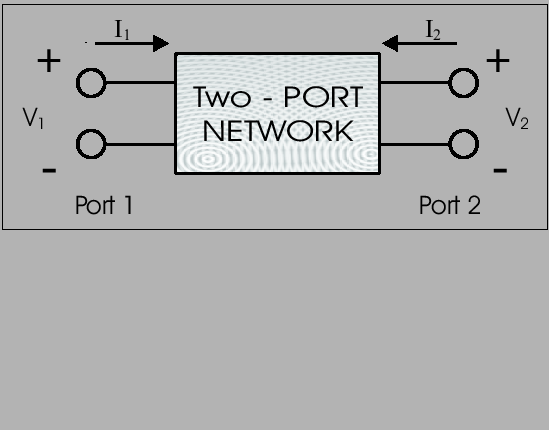 |
If the network is excited by voltage sources  and
and  ,
the network currents
,
the network currents  and
and  will be related to them
by the following equations:
will be related to them
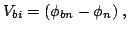
by the following equations:
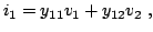 |
|
|
(2.68) |
 |
|
|
(2.69) |
where
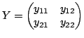 is called the admittance matrix.
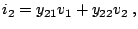
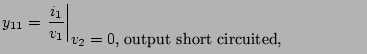
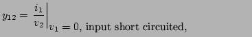
In the absence of additional information, four measurements are
required to determine the four parameters  ,
,  ,
,
 ,
,  . Each measurement is carried out with one port
of the network excited by a voltage source, while the other port
is short circuited, as better listed in the follows:
. Each measurement is carried out with one port
of the network excited by a voltage source, while the other port
is short circuited, as better listed in the follows:
 |
|
|
(2.70) |
 |
|
|
(2.71) |
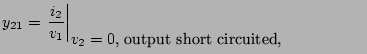 |
|
|
(2.72) |
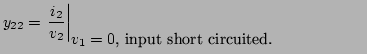 |
|
|
(2.73) |
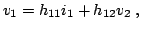
Very similar to the admittance matrix is the impedance matrix. If
the network is excited by current sources and , the
network voltages and will be related to them by
the following equations:
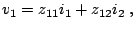 |
|
|
(2.74) |
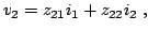 |
|
|
(2.75) |
where
 is called the impedance matrix.
In the absence of additional information, four measurements are
required to determine the four parameters  ,
,  ,
,
 ,
,  . Each measurement is carried out with one port
of the network excited by a current source while the other port is
open circuited, as better listed in the follows:
. Each measurement is carried out with one port
of the network excited by a current source while the other port is
open circuited, as better listed in the follows:
 |
|
|
(2.76) |
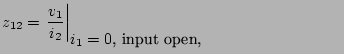 |
|
|
(2.77) |
 |
|
|
(2.78) |
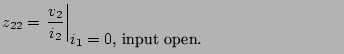 |
|
|
(2.79) |
It is easy to see how impedance and admittance matrix are related:
 |
(2.80) |
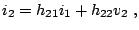
2.3.1.3 h-parameters
Slightly different to the admittance and impedance matrices (but
not less important as it will be shown in the next sections) is
the hybrid matrix. If the network is excited by input current
source and output voltage source , the network
output current  and the network input voltages will
be related to them by the following equations:
and the network input voltages will
be related to them by the following equations:
 |
|
|
(2.81) |
 |
|
|
(2.82) |
where
 is called the hybrid matrix.
In the absence of additional information, four measurements are
required to determine the four parameters  ,
,  ,
,
 ,
,  , as better listed in the following:
 |
|
|
(2.83) |
 |
|
|
(2.84) |
 |
|
|
(2.85) |
 |
|
|
(2.86) |
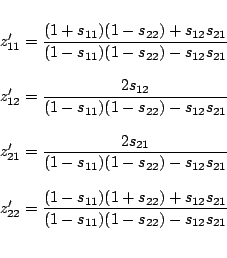
Table 2.1:
Parameter conversion table.
|
|
Even if all parameter sets contain the same information about a
network, and it is always possible to obtain any set from another
set (Table 2.1), scattering
parameters are important in microwave design, because they are
easier to measure at higher frequencies than the others. They are
conceptually simple, dimensionless, analytically convenient, and
capable of providing a great insight into a measurement or design
problem.
Scattering parameters are commonly called S-parameters; they
relate to travelling waves, which are scattered or reflected when
a n-port network is inserted into a transmission line. Their
definition, given by Kurokawa [Kur65], starts with the
normalized complex voltage waves:
 |
|
|
(2.87) |
 |
|
|
(2.88) |
In the available measurement systems, there is only a 2-port
network (i=1,2) and the reference impedances  are real and
equal to
are real and
equal to  (
( as described in the calibration
section).
as described in the calibration
section).
 |
(2.89) |
 |
(2.90) |
 |
(2.91) |
 |
(2.92) |
The linear equations describing the 2-port network are:
 |
|
|
(2.93) |
 |
|
|
(2.94) |
where
 is the matrix of the following S-parameter:
 |
(2.95) |
 |
(2.96) |
 |
(2.97) |
 |
(2.98) |
An oscillator can be considered as the combination of an active
multiport and a passive multiport (the embedding network). For the
active device, we have:
![$\displaystyle [V]=[Z][I] \thickspace ,$](http://web.tiscali.it/decartes/phd_html/img316.png) |
(2.99) |
and for the embedding network:
![$\displaystyle [V']=[Z'][I'] \thickspace .$](http://web.tiscali.it/decartes/phd_html/img317.png) |
(2.100) |
In our case, and  are the impedance matrixes of the
diode and of the passive elements.
are the impedance matrixes of the
diode and of the passive elements.
By connecting the active and the embedding network:
![$\displaystyle [I]=-[I'] \thickspace ,$](http://web.tiscali.it/decartes/phd_html/img319.png) |
(2.101) |
![$\displaystyle [V]=[V'] \thickspace ,$](http://web.tiscali.it/decartes/phd_html/img320.png) |
(2.102) |
and from Eq. (2.99) and
Eq. (2.100) results:
![$\displaystyle \{[Z]+[Z']\}[I]=0 \thickspace .$](http://web.tiscali.it/decartes/phd_html/img321.png) |
(2.103) |
Now since ![$ [I]\neq0$](http://web.tiscali.it/decartes/phd_html/img322.png) , the matrix [Z]+[Z'] is singular or
, the matrix [Z]+[Z'] is singular or
![$\displaystyle det([Z]+[Z'])=0 \thickspace .$](http://web.tiscali.it/decartes/phd_html/img323.png) |
(2.104) |
Equation 2.104 is the generalized
oscillation condition. Since Z is a function of the frequency and
of the voltage, the oscillating frequency can be determined for a
given bias point. It can be demonstrated that an equivalent
condition of Eq. (2.104) is [KO81]:
![$\displaystyle det([S][S'] -1) =0$](http://web.tiscali.it/decartes/phd_html/img324.png) |
(2.105) |
or in a similar way
![$\displaystyle det([Y] + [Y'])=0 \thickspace ,$](http://web.tiscali.it/decartes/phd_html/img325.png) |
(2.106) |
where  and
and  are the scattering and admittance matrices of
the diode and
are the scattering and admittance matrices of
the diode and  and
and  are the scattering and admittance
matrices for the passive elements, respectively. If maximum power
output and efficiency are not of prime importance, a satisfactory
oscillator design can be achieved using small-signal scattering
matrix parameters. The major shortcoming of small signal
oscillator design is that it does not provide any way of
predicting the steady-state oscillating signal level. Oscillator
design based on large-signal scattering matrix (i.e. non-linear)
parameters is much more complicated because of the difficulty of
obtaining large-signal parameters.
are the scattering and admittance
matrices for the passive elements, respectively. If maximum power
output and efficiency are not of prime importance, a satisfactory
oscillator design can be achieved using small-signal scattering
matrix parameters. The major shortcoming of small signal
oscillator design is that it does not provide any way of
predicting the steady-state oscillating signal level. Oscillator
design based on large-signal scattering matrix (i.e. non-linear)
parameters is much more complicated because of the difficulty of
obtaining large-signal parameters.
2.3.3 Gunn oscillation modes
In order to generate microwave power, a transferred electron
device has to be placed in a cavity or in a resonant circuit.
Several modes of operation can be distinguished. Each of them
provides particular advantages or disadvantages from the point of
view of tunability, stability and efficiency. The following four
main operation modes will be discussed [Hei71,Hob74]:
- the Transit Time mode,
- the Delayed Domain mode,
- the Quenched Domain mode,
- the LSA mode.
Figure 2.15:
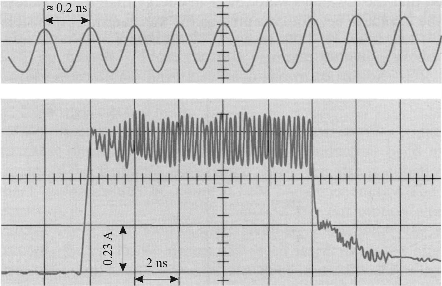
Current and voltage time evolution of the Gunn oscillator operating in the Transit Time mode.
|
|
In a purely resistive circuit, the oscillation frequency  is
determined by the space charge or domain transit time
is
determined by the space charge or domain transit time  :
:
 |
(2.107) |
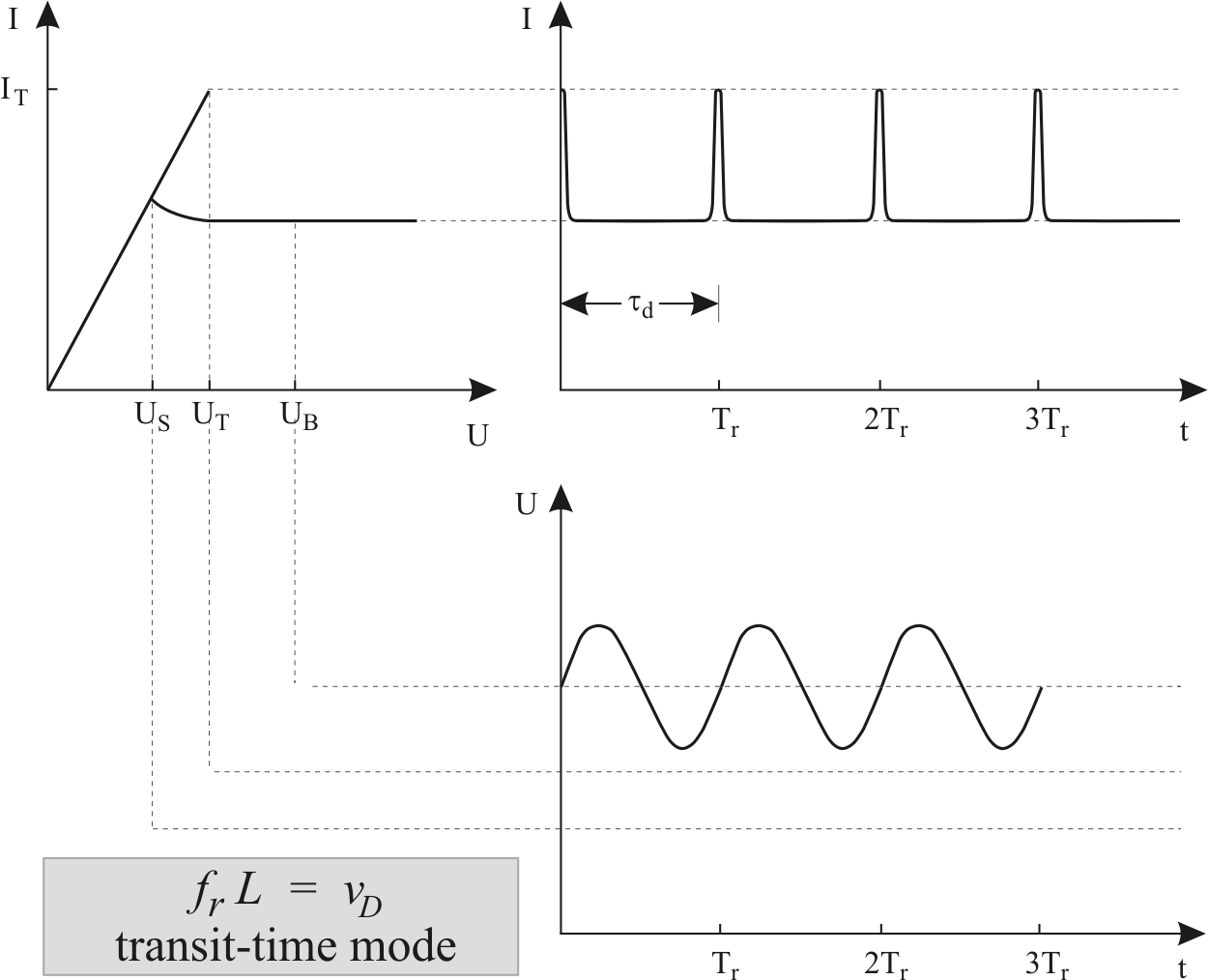
This operating mode is commonly called Transit Time mode. The
current flows with a sequence of short current pulses with the
period . The current spikes occur when a domain enters the
anode and the next one is originating from the cathode. The
voltage is sinusoidal with the same period
(Fig. 2.15). If the circuit is heavily
loaded, the R.F. voltage is small enough not to oscillate below
.
The efficiency of the Transit Time mode is not particularly high
because of the narrowness of the current pulse and the small r.f.
voltage amplitude. Moreover, the frequency range is fixed to the
natural domain transit frequency. This disadvantage influences
also the frequency stability, because the domain transit time is
strongly temperature dependant.
In this case, the resonant period of
the circuit  is longer than :
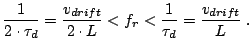 |
(2.108) |
Figure 2.16:
Current and voltage time evolution of the Gunn oscillator operating in the Delayed Domain mode.
|
|
The amplitude of the voltage sinusoidal waveform
(Fig. 2.16) has to be large enough to cause
the voltage to fall below threshold over a portion of the
cycle. The domain reaches the anode and disappears during the
second half of the voltage oscillation, while the voltage is below
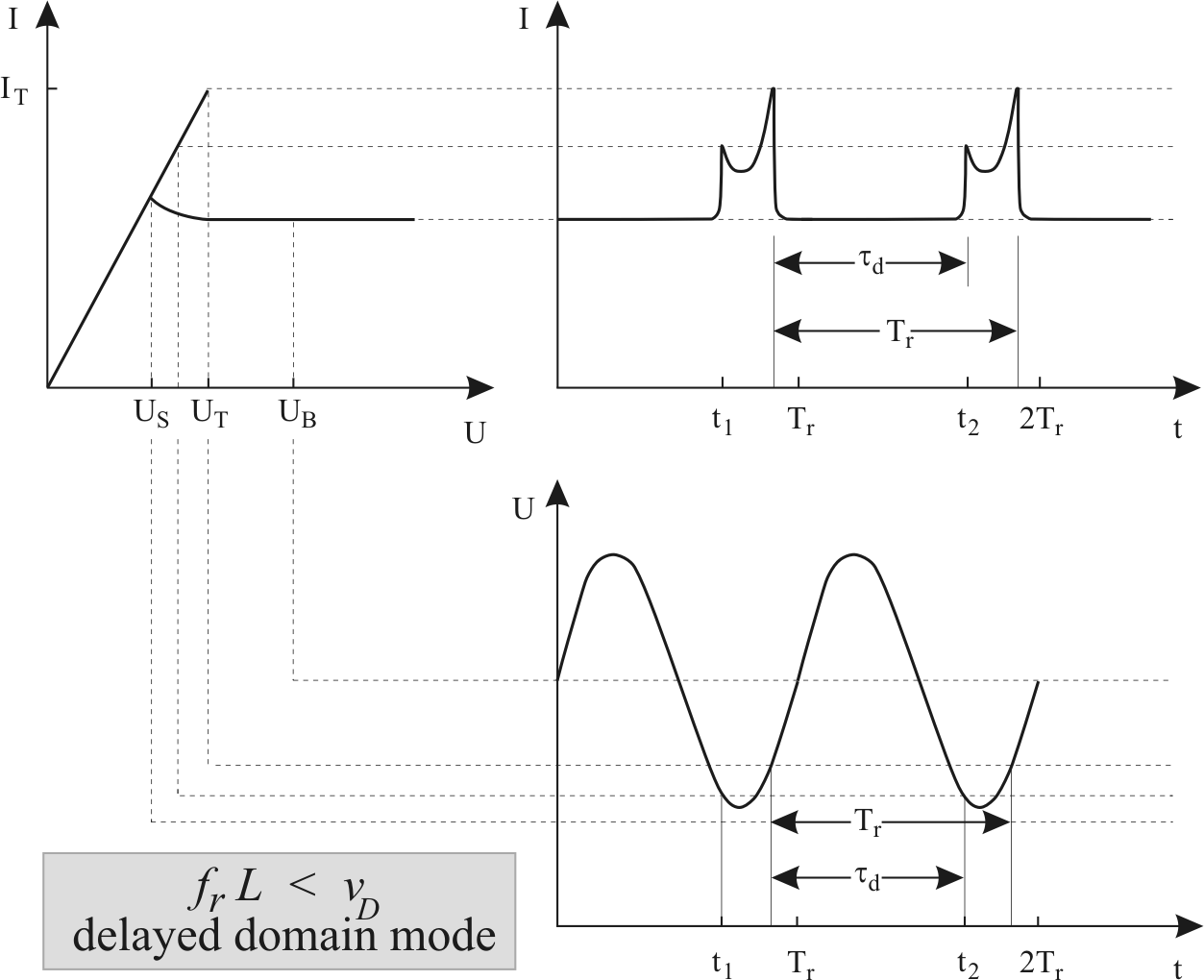
the threshold. Before the next domain can be nucleated, the
voltage has to rise again over the threshold. The efficiency of
the Delayed Domain mode is higher than for the Transit Time and,
thanks to the larger current pulses, can reach up to 7.2% [War66]. The frequency is controlled by the resonant circuit,
whose tunability can be mechanical or electrical (parallel
Schottky varactors). A good temperature stability is achieved,
generally, for aluminium cavities or DRO (Dielectric Resonator
Oscillators).
Figure 2.17:
Current and voltage time evolution of the Gunn oscillator operated in the Quenched Domain mode.
|
|
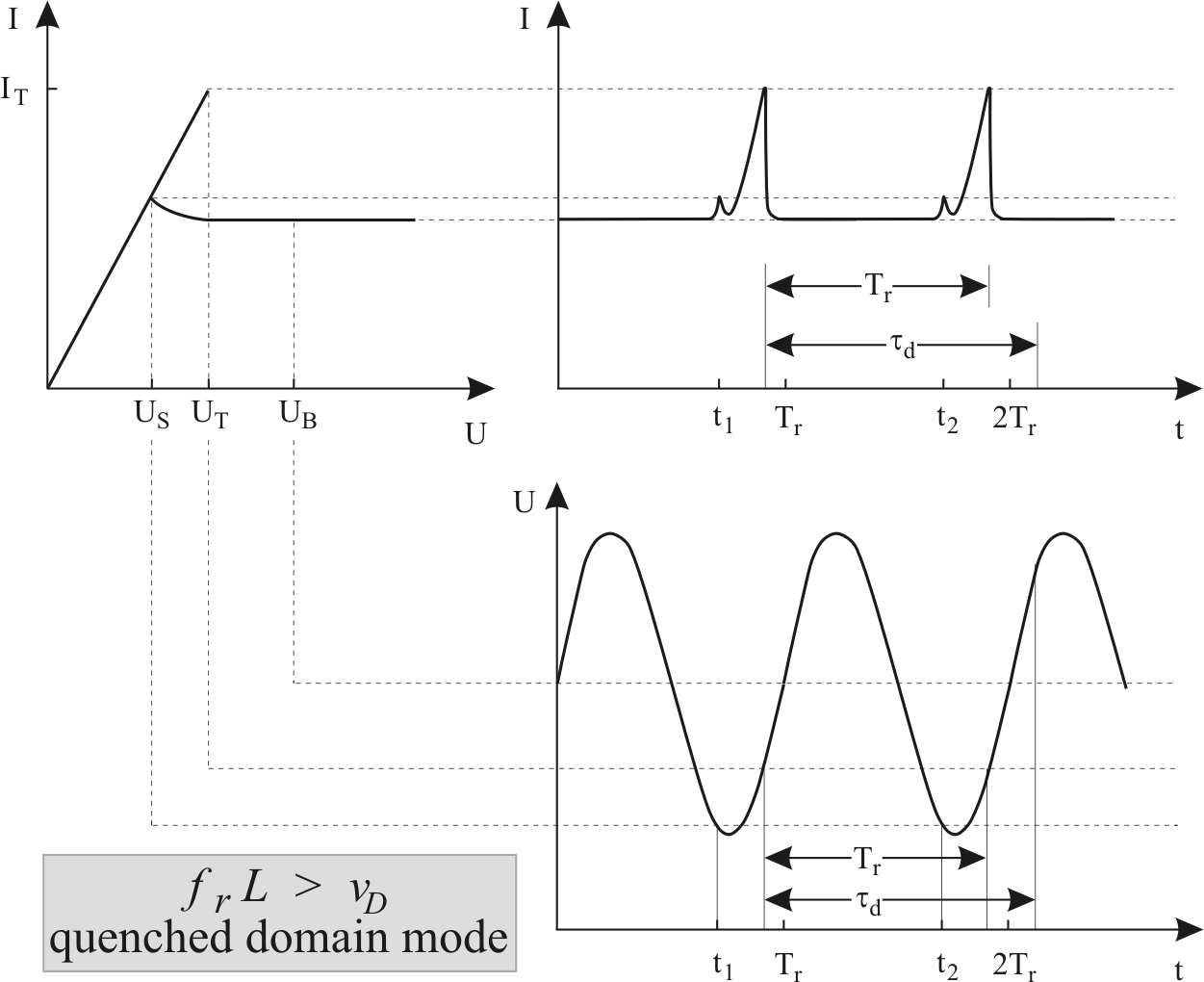
For this mode, the resonant period of the circuit is
shorter than , but longer than the domain nucleation and
extinction time  :
:
 |
(2.109) |
The circuit loading is further reduced and the voltage falls below
the domain sustaining voltage  for a portion of the cycle.
The domain is generated in the cathode and, before reaching the
anode, is quenched in flight, because the voltage falls below
. The next domain can not be nucleated until the terminal
voltage rises above the threshold . The main advantage of
this mode consists in the generation of frequencies higher than
the transit-time frequency. Considering the area under the
current-pulse, it is evident that the efficiency of the Quenched
Domain mode (5% [Hob74]) is higher than the one of the
Transit Time mode, but lower than the one of the Delayed Domain
mode.
for a portion of the cycle.
The domain is generated in the cathode and, before reaching the
anode, is quenched in flight, because the voltage falls below
. The next domain can not be nucleated until the terminal
voltage rises above the threshold . The main advantage of
this mode consists in the generation of frequencies higher than
the transit-time frequency. Considering the area under the
current-pulse, it is evident that the efficiency of the Quenched
Domain mode (5% [Hob74]) is higher than the one of the
Transit Time mode, but lower than the one of the Delayed Domain
mode.
2.3.3.4 The LSA mode.
It has been already anticipated, that a domain can be quenched
before reaching the anode, if the device bias falls below .
The lifetime of the domain is connected with the resonance
frequency of the circuit. If the frequency is high enough, the
domain will not have time to fully nucleate and the diode operates
in the LSA mode. LSA stands for Low Space-charge Accumulation. In
this context, the I-V characteristics of the device should follow
the v-E, which exhibits a region of negative differential mobility.
A first advantage of this mode consists in the high frequencies,
which are achievable: the device length is not related to the
oscillating frequency, which can be many times the transit time
frequency (overlength Gunn oscillator). The second
advantage concerns the R.F. output power: in the LSA mode, higher
terminal voltages may be applied without causing impact
ionizations [Hob74] and outstanding efficiencies up to 18.5%
are reported [Cop67b].
The performances of the LSA mode are limited by four practical
constraints to prevent the domain formation:
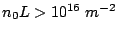
- The doping concentration divided by the frequency
 must remain in the interval
![$ [2\cdot10^{10},2\cdot10^{11}] \thickspace s
m^{-3}$](http://web.tiscali.it/decartes/phd_html/img339.png) (GaAs case) [Cop67b].
(GaAs case) [Cop67b].
- The homogeneity of the doping concentration and of the
related low field conductivity must be better than 10%
[Cop67b,Hob72].
- Not to distort the uniform-field conditions with the unavoidable accumulation layer, the device must be much longer than the space-charge
transit length per cycle.
- The oscillating circuit must be designed in a way to prevent a
long delay before starting the oscillation. During this delay,
a domain could nucleate and cause device breakdown by impact
ionization.
Figure 2.18 summarizes the operating
modes of a GaAs transferred electron device as a function of the
doping concentration, frequency and device length. Three different
situations can be distinguished: stable amplification, domain
oscillation and LSA oscillation.
For
 , no domain formation appears
and the device can be used as an amplifier in frequency ranges
around the transit frequency. For
, no domain formation appears
and the device can be used as an amplifier in frequency ranges
around the transit frequency. For
 three different domain oscillation modes are possible
depending on the resonator frequency: Transit Time, Delayed Domain
and Quenched Domain mode. For higher frequencies and for
three different domain oscillation modes are possible
depending on the resonator frequency: Transit Time, Delayed Domain
and Quenched Domain mode. For higher frequencies and for
![$ n_0/f
\in [2\cdot10^{10}, 2\cdot10^{11}] \thickspace sm^{-3}$](http://web.tiscali.it/decartes/phd_html/img343.png) , we have
the LSA mode.
, we have
the LSA mode.
The presented boundaries should not be regarded as absolute. The
device behaviour next to the boundaries is also depending on the
bias voltage, device temperature and circuit loading.
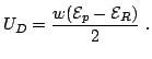
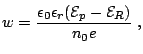
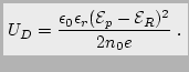
2.4 The thermal behaviour of a Gunn diode
In today's environment of high performance semiconductor devices,
the common complaints that it is possible to "cook an egg" or
"warm your coffee" on an electronic appliance like a typical
modern computer are not that far fetched. Many semiconductor
manufacturers have grappled with the difficulty of combining
highly evolved thermal dissipation techniques with the dual
requirement of packaging simplicity and reliability. In this
context, the problem of the Gunn diode cooling is crucial.
As illustrated in the previous chapters, the efficiency of a Gunn
diode is not very high. In order to achieve the required R.F.
output levels, D.C. power densities greater than
 are reached2.5. Therefore, in addition to good electric
contacts, the Gunn diode requires good thermal contacts to the
environment to avoid its destruction by overheating.
are reached2.5. Therefore, in addition to good electric
contacts, the Gunn diode requires good thermal contacts to the
environment to avoid its destruction by overheating.
The standard packaging consists in the removal of the heat
occurring from one end of the device with an integrated gold heat
sink. The heat-sink is electroplated on the semiconductor and then
bounded to a copper pedestal ultrasonically or by
thermocompression. Only for research purposes, sometimes copper
is replaced with diamond, for which the thermal conductivity at
room temperature is 30 times higher than copper.
In this work, an original quasi-planar double-sided heat-sinking
is presented: from the bottom side, the heat flows through the
semiconductor substrate and from the top side, thick gold
airbridges for electrical connections are exploited also as
heat-sink.
In this section after an analytical description of the thermal
problem, finite elemente simulations of the standard and the
double-sided heat-sink are compared. The efficiency of the top
contact heat-sink is presented here theoretically and in chapter
6 experimentally.
2.4.1 Analytical solution of the simplified static heat transfer problem
For most geometries, the detailed solution of the heat-flow
problem through a small active device in a massive heat-sink is
complicated.
Figure 2.19:
Approximation of the device geometry to simplify the heat transfer problem [Hob74].
|
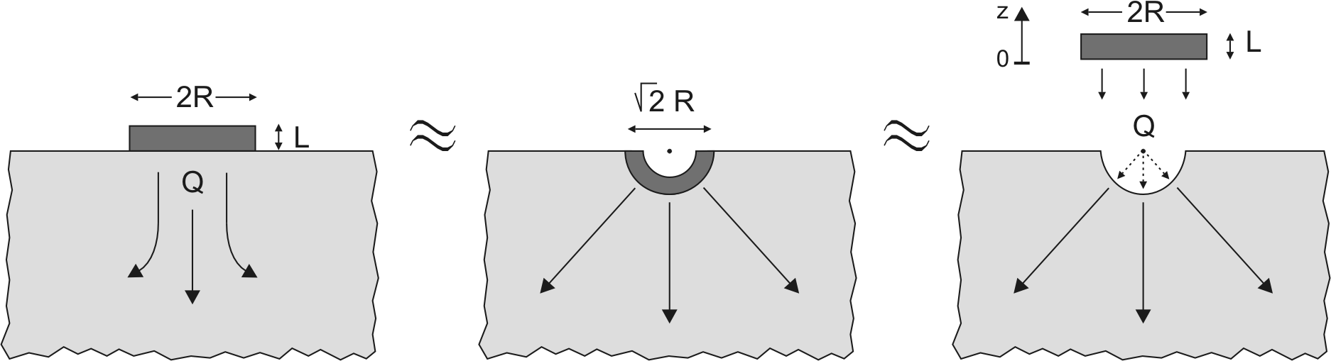
|
In the case of simple conduction2.6, the heat transfer equation is
given by:
 |
(2.110) |
where  is the power density of the heat source
 ![$ [Wm^{-3}]$](http://web.tiscali.it/decartes/phd_html/img349.png) and
and
 is the thermal conductivity2.7.
In order to achieve simple analytical solutions, some assumptions
are required. If interfacial and contact electrical resistances
are negligible, all the heat is dissipated in the active region of
the device. The composite geometry of the heat flow can be
simplified as shown in Fig. 2.19. The
Gunn device is considered as a series connection of a one
dimensional active device region and a heat-sink with spherical
symmetry heat flow.
The solution of of the first part of the heat flow problem for
the one dimensional active region (dark-gray
Fig. 2.19) with uniform heating is
well-known [Hob74]:
 |
(2.111) |
where  is the maximum temperature,
  is the
temperature at the border, is the diode length,
is the
temperature at the border, is the diode length,  is the
diode radius,
is the
diode radius,
 is the thermal conductivity of the
active region and
is the thermal conductivity of the
active region and
 is the dissipated
power. The solution of the second part of the problem (heat flow
in the heat-sink, light-gray Fig. 2.19))
,considering a point source and spherical symmetry, is given by
[Hob74]:
is the dissipated
power. The solution of the second part of the problem (heat flow
in the heat-sink, light-gray Fig. 2.19))
,considering a point source and spherical symmetry, is given by
[Hob74]:
 |
(2.112) |
where
 is the thermal conductivity of the heat-sink.
Combining together Eq. (2.111) and
Eq. (2.114), the complete heat flow equation is
 |
(2.113) |
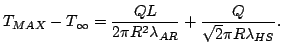
The thermal resistance  of the whole system Gunn diode and
heat-sink is:
of the whole system Gunn diode and
heat-sink is:
 |
(2.114) |
Equation 2.113 confirms that, for a given
device length, it is preferable to have the radius R as large as
possible. At the same time, in order to keep the electrical
resistance constant, the device resistivity must increase. The
resistivity is depending on the electron concentration. However,
too low doping concentrations have to be considered with caution,
in order to avoid low rf efficiencies.
Another important factor for Eq. (2.113) is the
thermal conductivity: it depends extremely of material. The active
region thermal conductivity for GaAs, InP and GaN are:
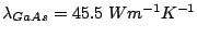 ,
,
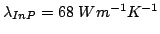 and
and
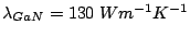 . The excellent value of GaN are compensated by the
power density, which this material requires before having
transferred electron effects. Crucial for reducing the thermal
resistance is also the material choice of the heat-sink.
Materials, which are often used, are: copper (
. The excellent value of GaN are compensated by the
power density, which this material requires before having
transferred electron effects. Crucial for reducing the thermal
resistance is also the material choice of the heat-sink.
Materials, which are often used, are: copper (
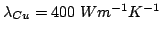 ), gold (
 ) and diamond (
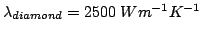 ).
).
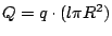
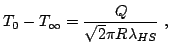
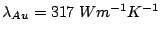
As an example, the temperature within the GaAs is computed for the
case of an integrated gold heat-sink. A diode length of
 and a radius R of
 have
been considered with a dissipated power of Q =
have
been considered with a dissipated power of Q =
 .
For an environment temperature of
.
For an environment temperature of
 =
=  K,
the resulting maximal temperature within the device is
K,
the resulting maximal temperature within the device is
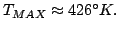 |
(2.115) |
Replacing the gold heat-sink with a GaAs substrate, it follows
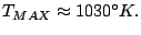 |
(2.116) |
Without heat-sink, the temperature is more than the double and
the diode would be destroyed immediately.
2.4.2 Finite elemente simulations of the temperature distributions in a Gunn diode
The problem of the heat flow in Gunn diodes has been solved
numerically with the commercial software Finite Element
Method Laboratory. FEMLAB is a modelling package for the
simulation of physical processes, which can be described via
partial differential equations. The modelling activity is a
sequence of four steps:
- Create the diode geometry with a 3D CAD environment.
- Define the physics of the heat flow including the necessary
material parameters.
- Generate the finite elemente mesh.
- Compute and analyze the solution.
The simulation has been performed on two structures: a
conventional Gunn diode chip and a quasi-planar Gunn diode with
air-bridges.
The Gunn diode chip is composed of a cylindrical top gold contact
with a diameter of
 , a GaAs mesa with the
same area and a conventional bottom heat-sink. The heat-sink
consists of a cylindrical gold contact with a diameter of
, a GaAs mesa with the
same area and a conventional bottom heat-sink. The heat-sink
consists of a cylindrical gold contact with a diameter of
 and a height of
 , laying
on top of a copper block with a diameter of
, laying
on top of a copper block with a diameter of
 and a height of
 . As a boundary
condition, the outer faces of the whole structure are kept
thermally isolated, except for the copper bottom face, which is
kept at a constant temperature of
. As a boundary
condition, the outer faces of the whole structure are kept
thermally isolated, except for the copper bottom face, which is
kept at a constant temperature of
 .
.
The quasi-planar Gunn diode is composed of a GaAs mesa on top of a
thick GaAs substrate. The top face of the
mesa (
 ) is connected with
 thick gold air-bridges to the substrate at a
distance of
thick gold air-bridges to the substrate at a
distance of
 . The same boundary conditions
have been chosen: the outer faces of the whole structure are
thermally isolated, except for the GaAs substrate bottom face,
which is kept at a constant temperature of
.
. The same boundary conditions
have been chosen: the outer faces of the whole structure are
thermally isolated, except for the GaAs substrate bottom face,
which is kept at a constant temperature of
.
In both cases, the GaAs mesa is divided into a
active layer with a constant uniform power dissipation
(
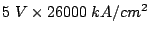 ) and two
contact layers of
) and two
contact layers of
 . No irradiation process has
been considered.
. No irradiation process has
been considered.
The results of the simulations are presented in
Fig. 2.20 - 2.23.
In Fig. 2.20 and in
Fig. 2.21, the temperature distribution is
shown for the Gunn diode chip and for the quasi-planar Gunn diode,
respectively. A 3D and a cross-sectional view of the two
structures visualises the different temperature regions by means
of different color levels. The maximal temperature reached by the
Gunn diode chip is
 . This result agrees well with
similar computations (
. This result agrees well with
similar computations (
 ) reported by Cords and
Förster [CF02]. In the case of the quasi-planar Gunn
diode, a higher temperature is expected, considering the poor
thermal conductivity of the GaAs substrate. Surprisingly, the
maximal temperature is only nine degree higher (
) reported by Cords and
Förster [CF02]. In the case of the quasi-planar Gunn
diode, a higher temperature is expected, considering the poor
thermal conductivity of the GaAs substrate. Surprisingly, the
maximal temperature is only nine degree higher (
 ): the gold air-bridges spread the heat from the top
increasing the interface area between the diode and the GaAs
substrate. The thicker the gold air-bridges, the better the
top-side cooling.
): the gold air-bridges spread the heat from the top
increasing the interface area between the diode and the GaAs
substrate. The thicker the gold air-bridges, the better the
top-side cooling.
In Fig. 2.22 and in
Fig. 2.23, the heat flux profile is
presented: the background color and the size of the cones are
proportional with the heat flux intensity. For the Gunn diode
chip, the maximal heat flux is close to the border of the active
region at the interface between GaAs and gold. The maximal flux
intensity of
 again agrees well with
Cords' and Förster's result of
again agrees well with
Cords' and Förster's result of
 .
.
For the quasi-planar Gunn diode, a high heat-flux is located at
the border of the active region at the interface with the GaAs
substrates. This region seams to be material independent, since a
similar zone can be seen in the Gunn diode chip. Anyway, the
highest heat flux values can be found in the arms of the gold
air-bridges, confirming the important role, which they have in
planar Gunn diodes.
Figure 2.20:
Heat-sink temperature profile for a standard Gunn diode chip.
|
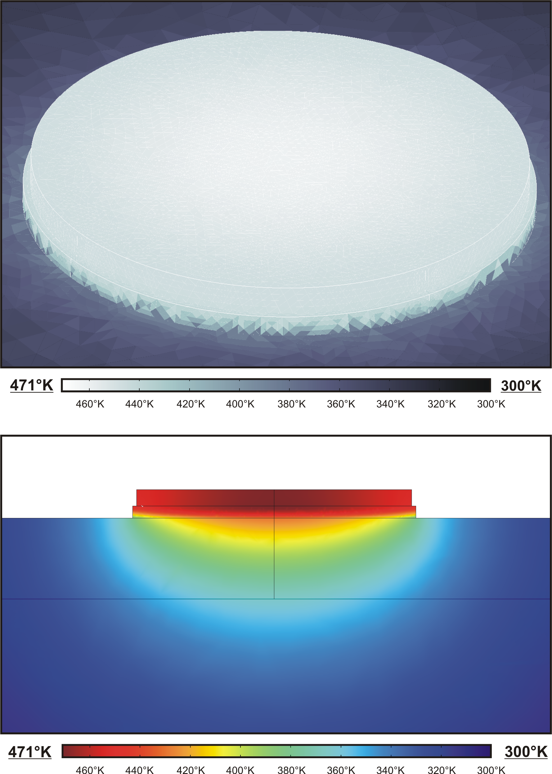
|
Figure 2.21:
Double-sided heat-sink temperature profile for a quasi-planar Gunn diode.
|
|
Figure 2.22:
Heat flux profile for a standard Gunn diode chip.
|
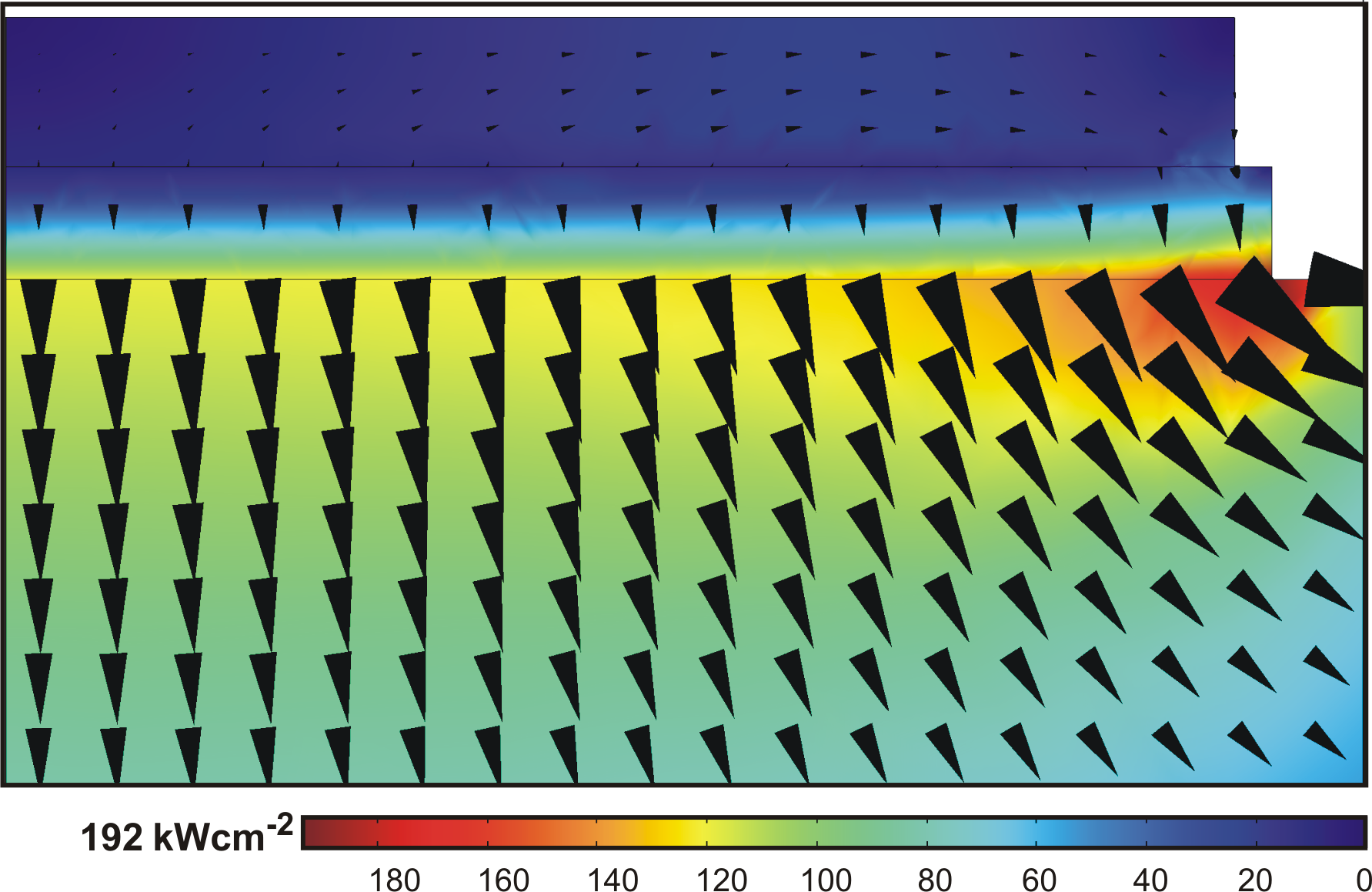
|
Figure 2.23:
Heat-flux profile for a quasi-planar Gunn diode.
|
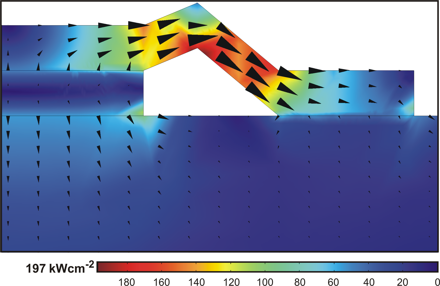
|
simone.montanari(at)tiscali.it
2005-08-02