Next: 7. Conclusions Up: Fabrication and characterization of Previous: 5. Technology Contents
The available ohmic contact technology (section
5.2 [Lep97,Jav03]) did not require any
improvement or optimization. However, TLM and CLM measurements
(see section 4.5) have been systematically performed
as quality verification to detect the process reproducibility or
irregularity. The contact pads of the TLM structures are
![]() squares and are separated by
increasing distances of 5, 10, 15, 20, 40, 80 and 120
squares and are separated by
increasing distances of 5, 10, 15, 20, 40, 80 and 120
![]() . The six circular shaped CLM structures consist of outer
circles with constant diameter of 100
. The six circular shaped CLM structures consist of outer
circles with constant diameter of 100
![]() and
concentric inner circles with a decreasing diameters of 96, 92,
88, 84, 80 and 68
and
concentric inner circles with a decreasing diameters of 96, 92,
88, 84, 80 and 68
![]() .
.
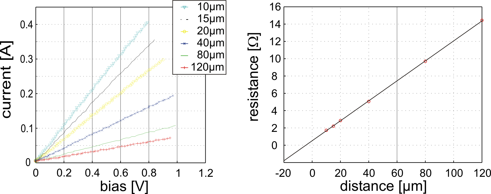 |
A measurement example for a TLM structure is shown in figure
6.1. The different linear I-V characteristics
(Fig. 6.1 left side) are depending on the distance
between pads. The interpolation of the resistance dependance on
the contact distance (Fig. 6.1 right side) provides
the contact resistance
![]() , the
effective contact length
, the
effective contact length
![]() , the specific
contact resistance
, the specific
contact resistance
![]() and
the sheet resistance
and
the sheet resistance
![]() .
.
All these parameters are summarized in table 6.1 for
different wafers.
| W-number | |||||
|
|
|
|
|||
| 17008 | GaAs | 0.047 | 2.7 |
|
17.6 |
| 18006 | GaAs | 0.040 | 2.3 |
|
17.4 |
| 18038 | GaAs | 0.038 | 2.2 |
|
17.5 |
| 19032 | GaAs | 0.038 | 2.1 |
|
17.9 |
| G695E2t | GaN | 0.165 | 0.7 |
|
238 |
| G695E2b | GaN | 0.097 | 2.0 |
|
48 |
Concerning GaAs, the specific contact resistance ![]() remains
under
remains
under
![]() , which defines the upper limit for
good ohmic contacts. The differences between the GaAs results are
due to the process reproducibility and on the slightly
different doping concentration of the considered wafers.
, which defines the upper limit for
good ohmic contacts. The differences between the GaAs results are
due to the process reproducibility and on the slightly
different doping concentration of the considered wafers.
The values for GaN, instead, refer to the same wafer G695 and to
the same sample E2. They have been prepared and annealed in the
same time. The only difference is that G695E2t was processed on
the top GaN contact layer and that G695E2b was processed on the
bottom contact layer. Even if the doping nominal level is the same
for the two layers, the top one is thinner than the bottom one
(
![]() vs.
vs.
![]() ); this could explain
the lower values of G695E2b sheet resistance. Another aspect that
should be taken into account, is the influence of the dry etching
and the related crystal deterioration: the bottom ohmic contact
G695E2b lays on a surface which was subjected to an aggressive
chlorine based plasma process. An improved plasma etching process
could reduce the reported inconsistency between top and bottom
contacts.
); this could explain
the lower values of G695E2b sheet resistance. Another aspect that
should be taken into account, is the influence of the dry etching
and the related crystal deterioration: the bottom ohmic contact
G695E2b lays on a surface which was subjected to an aggressive
chlorine based plasma process. An improved plasma etching process
could reduce the reported inconsistency between top and bottom
contacts.
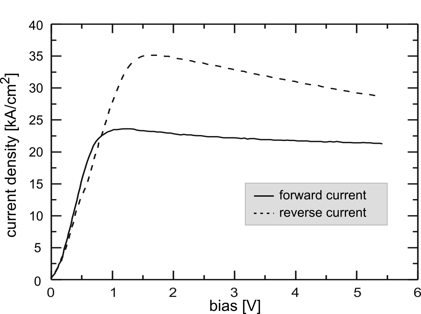
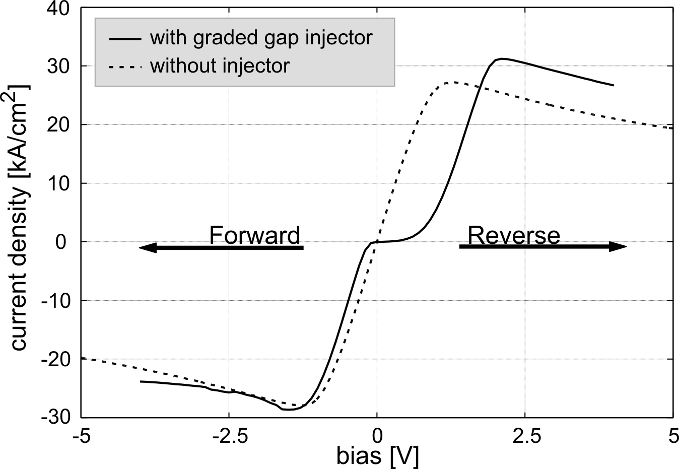
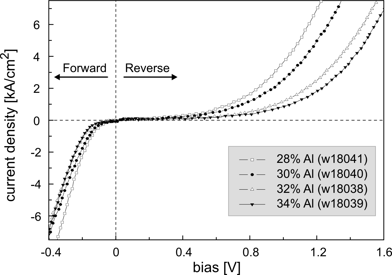
Figure 6.2 shows the DC characteristics of two GaAs Gunn diodes: one with the graded gap injector (GGI) and the other one without. In our case, the current flows in the forward direction when a negative voltage is applied on top of the device. As expected, the I-V characteristics of the diode without injector is symmetric. The diode with the graded gap injector presents an asymmetric I-V curve with a well pronounced Schottky-like behavior. In addition, the maximum current in the reverse direction (positive voltages) is about 10% higher than in the forward one. This is an indication for different electron occupations of the L-valley, causing different drift velocities for the two current directions.
|
|
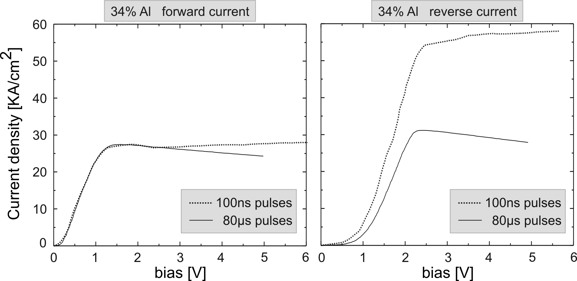
In order to find the most effective injector, devices with different maximum aluminium concentrations have been compared (28%Al up to 34%Al). The DC characteristics of the diodes for low voltages are shown in Fig. 6.3: especially in the reverse direction, the Schottky-like behavior becomes more pronounced with increasing Al concentration, i.e. higher barriers.
In the steep increasing part of the I-V curves, the slopes in the two directions are nearly identical. These slopes reflect the quality of the ohmic contacts and no relevant change has been observed for different Al concentrations in the barriers.
After the linear region, the current peak and the DC negative differential resistance should be interpreted as a pure self heating effect. Considering the poor heat properties of GaAs, self heating is playing an important role (see section 6.1.6 and section 6.2.1).
In the reverse current direction, electrons enter the active-region directly without passing any hot electron injector. In this case, no enhanced L-valley occupation can be expected. This results in a current peak nearly independent of the Al-concentration.
In the forward direction, different injectors lead to different
occupations of the L-valley and therefore to different peak drift
velocities and peak currents. The forward current decreases with
increasing Al concentration. The ratios between the peak current
densities ![]() in both directions are presented in Table
6.2.
in both directions are presented in Table
6.2.
| 28% Al | 30% Al | 32% Al | 34% Al | ||
| <#17373#> | 30.40 | 29.60 | 28.80 | 28.40 | |
| 31.05 | 31.20 | 30.60 | |||
|
|
0.98 | 0.95 | 0.94 | 0.92 | |
The current maxima in the forward and in the reverse direction can
be used as a measure of the injector effectiveness. The lower the
ratio
![]() , the more efficient is the electron
injection in the L-valley (Table 6.2).
Nevertheless, only a high frequency investigation allows an
analysis of the Gunn diode injector in the whole operating bias
range (
, the more efficient is the electron
injection in the L-valley (Table 6.2).
Nevertheless, only a high frequency investigation allows an
analysis of the Gunn diode injector in the whole operating bias
range (
![]() ), obtaining a quantitative estimation of the related L-valley
occupations (see section 6.2.4).
), obtaining a quantitative estimation of the related L-valley
occupations (see section 6.2.4).
|
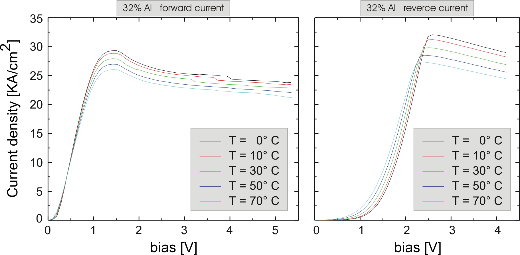
For low voltages, we assist to the opposite phenomena: the current increases rising the temperature. The low voltage behavior is extremely influenced by the injector: the thermionic emission of the electrons over the barrier increases dramatically with increasing temperatures.
In chapter 2.2.2, the equivalent circuit for a graded gap injector Gunn diode has been described and Eq. (2.60) has been proposed for analytical modelling. A simulation package for an automatic evaluation of temperature dependent I-V characteristics in connection with Eq. (2.60) has been written. A complete description of the methods and the software code can be found in [FML03].
Using Eq. (2.60) and taking as fitting
parameters ![]() ,
, ![]() and
and ![]() , the measured I-V curves have
been fitted at different temperatures (left diagram of
Fig. 6.5). For each temperature, a set of
, the measured I-V curves have
been fitted at different temperatures (left diagram of
Fig. 6.5). For each temperature, a set of ![]() ,
,
![]() and
and ![]() has been obtained.
has been obtained.
|
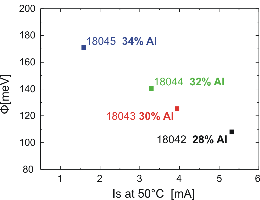
The described procedure has been applied to several diodes with
different injectors. For a better visualization of the results,
only four cases are considered, focusing on the influence of the
maximum Al concentration in the graded barrier. The diode layer
structures have been grown in a sequence and processed
simultaneously to minimize inaccuracy or inhomogeneity. In
Fig. 6.6, the barrier height ![]() is
represented as a function of the saturation current
is
represented as a function of the saturation current ![]() at
at
![]() C.
C.
|
The general tendency in Fig. 6.6 follows the expectations. Increasing the maximum Al concentration in the graded barrier, the saturation current decreases and the barrier height increases.
Once the layer-structure is decided and the parameters ![]() ,
,
![]() and
and ![]() are determined, the described procedure is
suggested as a production benchmark. In a global environment,
where costs and quality issues are strongly connected, minimum
reliability targets lower then 2ppm6.1 are standard requirements. Each
production step is a potential thread for the fulfillment of these
severe targets and needs a constant control. The proposed
benchmark gives a full overview on the layer structure and
processing quality with a small effort (DC measurements).
are determined, the described procedure is
suggested as a production benchmark. In a global environment,
where costs and quality issues are strongly connected, minimum
reliability targets lower then 2ppm6.1 are standard requirements. Each
production step is a potential thread for the fulfillment of these
severe targets and needs a constant control. The proposed
benchmark gives a full overview on the layer structure and
processing quality with a small effort (DC measurements).
Applying higher voltages, the current shows a peak and a negative
slope witnesses the self heating of the device. As for the GGI
Gunn diode, the forward current peak is much lower than the
reverse one. This is a first hint of the resonant tunneling
injector effectiveness. The already defined ratio between the peak
current density in the forward (
![]() ) and in
the reverse direction(
) and in
the reverse direction(
![]() ),
),
![]() is equal to 0.7. In comparison with the graded
gap injector (0.9), this is a much better result. Moreover, the
negative slope of the RTI diode in the forward direction is
flatter than the one in the reverse: this gives the impression of
a less influence of the forward current by self-heating effects.
is equal to 0.7. In comparison with the graded
gap injector (0.9), this is a much better result. Moreover, the
negative slope of the RTI diode in the forward direction is
flatter than the one in the reverse: this gives the impression of
a less influence of the forward current by self-heating effects.
One final remark for the RTD specialists concerns the resonance of
the double barrier and the peak to valley ratio. Figure
6.7 does not show any steep negative differential
resistance (typical in RTD structures) because of the particular
design of the device. The peak current of the isolated double
barrier structure has been estimated at current densities higher
than ![]() . The Gunn diode active region prevents the
flowing of such a high current and avoids the undesirable
bistability. For thick AlAs double barriers (
. The Gunn diode active region prevents the
flowing of such a high current and avoids the undesirable
bistability. For thick AlAs double barriers (![]() 6 monolayers),
such a phenomenon is expected in the following conditions: the
measurement has to be carried out at lower temperatures, with very
short pulses, and in the reverse direction, where the Gunn diode
current densities are higher.
6 monolayers),
such a phenomenon is expected in the following conditions: the
measurement has to be carried out at lower temperatures, with very
short pulses, and in the reverse direction, where the Gunn diode
current densities are higher.
Which is the real origin of the current saturation shown in
Fig. 6.8? Is the intervalley transfer playing a role in
this phenomenon? Concerning this aspect, it is difficult to make a
real comparison of the DC properties of the presented GaN Gunn
diode with data from the literature. Considering the threshold
field ![]() as the electric field at witch the slope of I-V is
zero, values of about
as the electric field at witch the slope of I-V is
zero, values of about
![]() can be estimated (
can be estimated (
![]() long pulses). This value is from 30% up to
40%, lower than the simulated values reported in the literature
[KOB+95,AWR+98]. The discrepancy could be explained as
misinterpretation of the device length (the active region has been
considered
long pulses). This value is from 30% up to
40%, lower than the simulated values reported in the literature
[KOB+95,AWR+98]. The discrepancy could be explained as
misinterpretation of the device length (the active region has been
considered ![]() long in the previous estimation).
long in the previous estimation).
The maximal current density levels are around
![]() . Taking as reference value typical GaAs Gunn diodes
without injector, the maximal current densities range from 30 to
. Taking as reference value typical GaAs Gunn diodes
without injector, the maximal current densities range from 30 to
![]() . The current density differences are due
to the different doping concentrations (
. The current density differences are due
to the different doping concentrations (
![]() for GaN and
for GaN and
![]() for GaAs) and
to the respective maximal drift velocities, which were already
described in chapter 2.1.2 and in
Fig. 2.4.
for GaAs) and
to the respective maximal drift velocities, which were already
described in chapter 2.1.2 and in
Fig. 2.4.
|
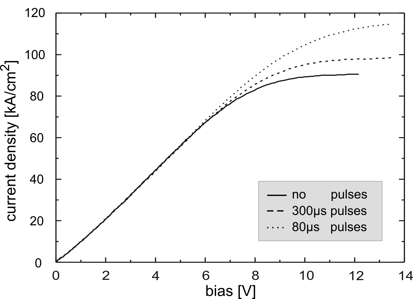
In Fig. 6.9, the I-V characteristics of a graded gap
injector Gunn diode with very short pulses (100ns) are
illustrated. For comparison, measurement carried out with longer
pulses (80![]() ) are also presented. It can be noticed, that
with short pulses, the I-V curves do not show a negative slope.
80
) are also presented. It can be noticed, that
with short pulses, the I-V curves do not show a negative slope.
80![]() pulses, instead, are enough long to heat up the diode.
This confirms, beyond doubt, that self heating is the origin of
the negative slope in the I-V characteristics of the Gunn diodes.
A better estimation of the negative slope dependance on the
heating time (pulse length) is
given in section 6.2.1.
pulses, instead, are enough long to heat up the diode.
This confirms, beyond doubt, that self heating is the origin of
the negative slope in the I-V characteristics of the Gunn diodes.
A better estimation of the negative slope dependance on the
heating time (pulse length) is
given in section 6.2.1.
In the forward current direction, up to the current peak, there is
practically no difference between long and short pulse I-V curves;
after the current peak, the difference remains marginal. For the
reverse bias, however, there is a large difference between the two
cases. The current increase is dramatic when the short pulses are
applied. The above evidences demonstrate the effectiveness of the
injector. In the reverse direction, the electron occupation of the
![]() valley is high. A long pulse length causes a stronger
self-heating of the active region leading to a higher inter-valley
transfer, a lower
valley is high. A long pulse length causes a stronger
self-heating of the active region leading to a higher inter-valley
transfer, a lower ![]() valley occupation and a lower mean
drift velocity. In the forward direction, the
valley occupation and a lower mean
drift velocity. In the forward direction, the ![]() valley
occupation is low because of the injector; a further decrease due
to the heating has only
marginal effects on the current.
valley
occupation is low because of the injector; a further decrease due
to the heating has only
marginal effects on the current.
The ratio between the peak currents in the two directions is now
free from self-heating effects and can give a clear estimation of
the injector effectiveness.
The short pulse setup was also used to determine the breakthrough
voltage for diodes with different injectors and with different
passivation [Pro04]. The breakthrough voltage is indicated by
a sudden increase in the current behavior for high biases.
Measuring the breakthrough voltage with long pulses, it damages
irreversibly the Gunn diodes, due to the current stress. With
short pulses, the influence of a ![]() passivation has been
examined. The average value of the measured breakthrough voltages
is about 9V. Negligible differences have been found between
passivated and unpassivated diodes. As expected, the breakthrough
voltage is slightly higher in the forward direction because of the
lower current density.
passivation has been
examined. The average value of the measured breakthrough voltages
is about 9V. Negligible differences have been found between
passivated and unpassivated diodes. As expected, the breakthrough
voltage is slightly higher in the forward direction because of the
lower current density.
|
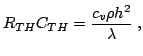
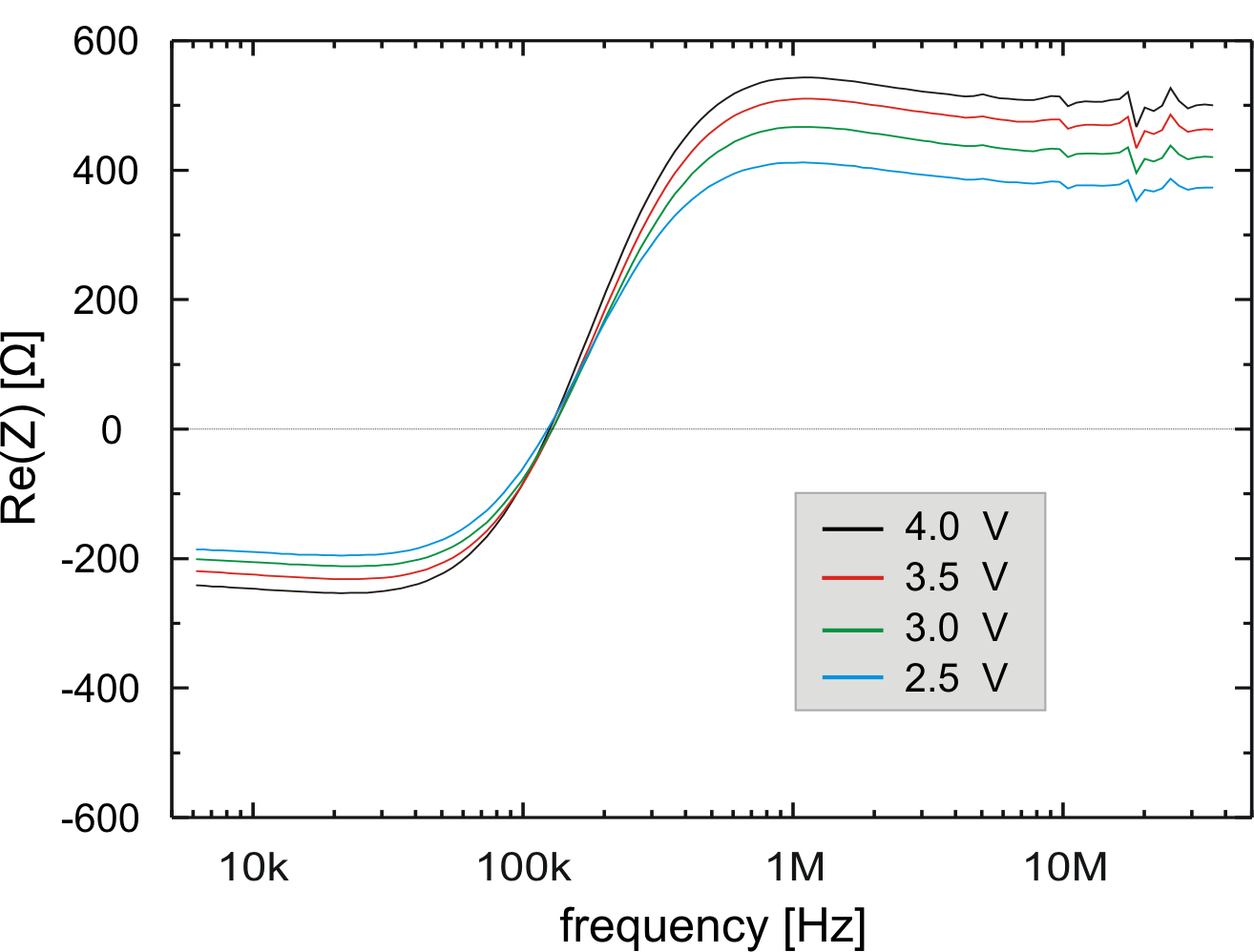
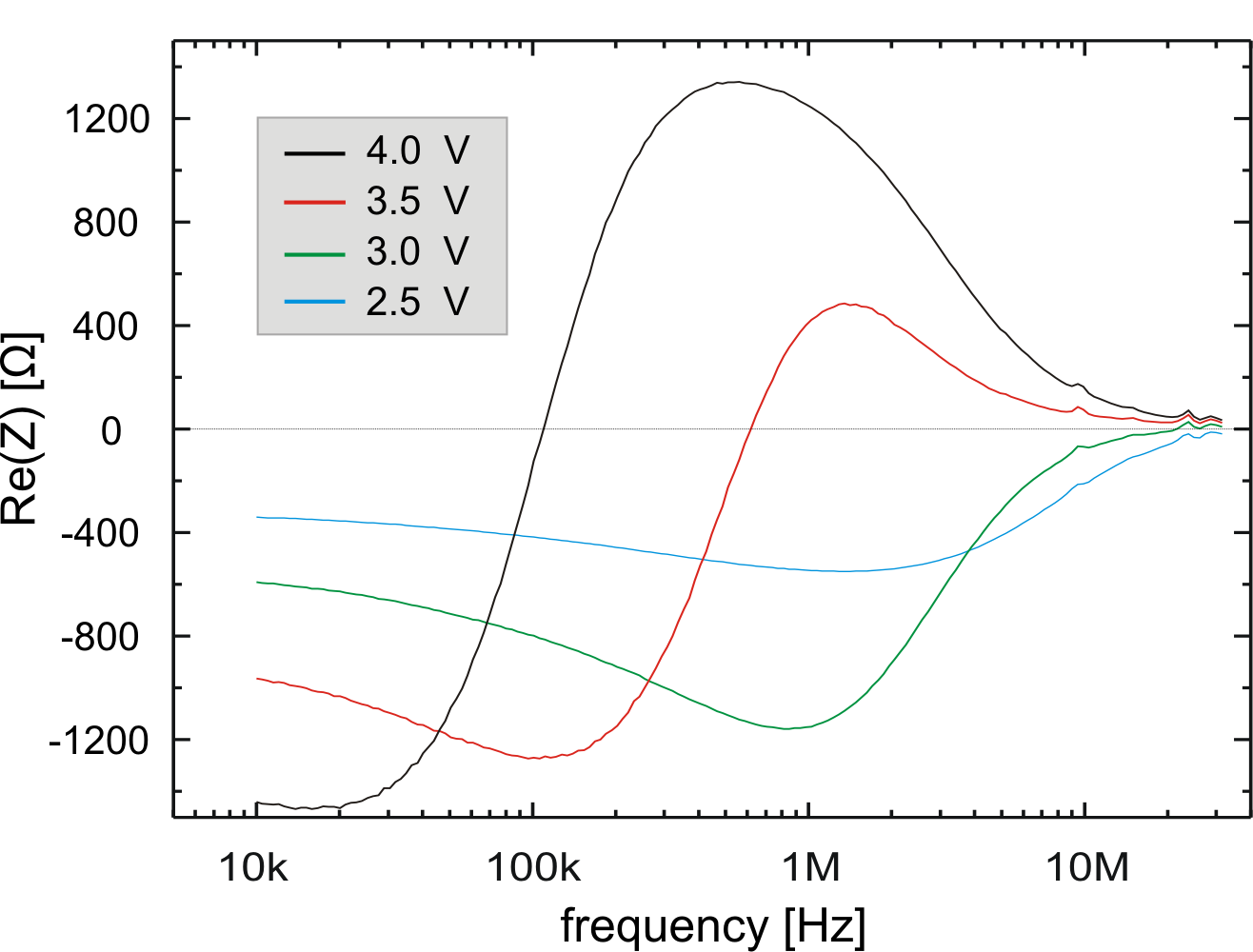
In Fig. 6.10, the real part of the measured
impedance is presented as function of the frequency for a GaAs
Gunn diode without injector. The absolute value of the
differential resistance increases for increasing bias voltages.
For all the biases, the transition from negative to positive
differential resistances appears at a frequency between 100 and
![]() . This transition can be better understood
introducing an equivalent circuit for the temperature changes
inside the diode. The thermal resistance and capacity of the Gunn
diode mesa are defined as:
. This transition can be better understood
introducing an equivalent circuit for the temperature changes
inside the diode. The thermal resistance and capacity of the Gunn
diode mesa are defined as:
| (6.2) | |||
| (6.3) |
 |
(6.4) | ||
 |
(6.5) |
| (6.6) |
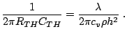
For our GaAs mesa ![]() is
is
![]() ,
, ![]() is
is
![]() ,
, ![]() is
is
![]() and h
is
and h
is
![]() .
. ![]() can be estimated as:
can be estimated as:
| (6.9) |
| (6.10) |
Impedance measurements have been also performed on graded gap
injector GaAs Gunn diodes. A Gunn diode with a hot electron
injector does not follow anymore the described model. The heating
of the device is not uniform. Furthermore, the dissipated power
density distribution is depending on the voltage. In
Fig. 6.11, it can be noticed that the transition
frequency changes with voltage. At
![]() the
transition frequency is between 100 and
the
transition frequency is between 100 and
![]() , like
for the diodes without injector. For lower voltages, the
transition frequency shifts to much higher frequencies.
, like
for the diodes without injector. For lower voltages, the
transition frequency shifts to much higher frequencies.
|
To understand Fig. 6.11 and the injector influence,
let us consider a diode bias range from 2 up to
![]() . If we assume the current to be constant after the threshold
voltage, the power dissipated in the injector is also constant. In
the same bias range, the diode dissipated power increases linearly
with the terminal voltage. From these considerations, at higher
voltages, the influence of the injector can be almost neglected,
explaining the similarity found at
. If we assume the current to be constant after the threshold
voltage, the power dissipated in the injector is also constant. In
the same bias range, the diode dissipated power increases linearly
with the terminal voltage. From these considerations, at higher
voltages, the influence of the injector can be almost neglected,
explaining the similarity found at
![]() between diodes
with and without injector.
between diodes
with and without injector.
|
Gunn diodes are normally mounted in a cavity and the resulting oscillators are measured and used as microwave generators. The literature of the last 30 years deals extensively with such data. Despite the possibility to de-embed the package, the cavity and the outside circuit from the measured data, it is very hard to achieve a good characterization of the device. The resulting information does not help to explain completely the behavior of the diode itself. Therefore, S-parameter measurements up to 110 GHz have been performed, in order to evaluate the small signal behavior of Gunn diodes with and without hot electron injector, at very high frequencies.
A complete description of the S-parameters and of the network analyzer setup can be found respectively in chapter 2.3.1 and 4.7.1.
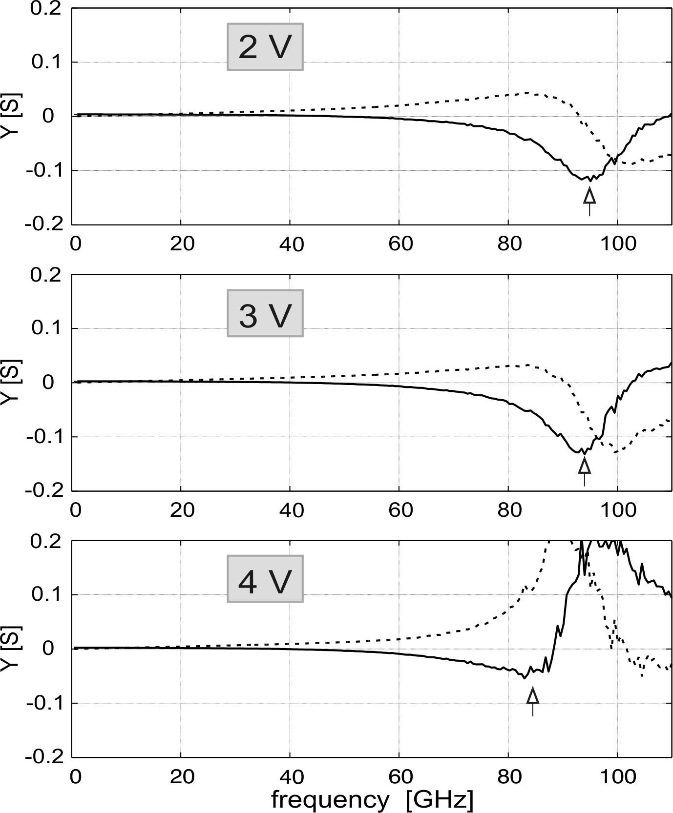
The conductance and the susceptance of a Gunn diode without
injector for different positive bias voltages are shown in
Fig. 6.12. The negative conductance presents a
voltage dependent minimum. The corresponding frequencies are 96
GHz at
![]() , 92 GHz at
, 92 GHz at
![]() and 87 GHz
at
and 87 GHz
at
![]() . In all the measured samples, the negative
conductance minima frequency decreases with increasing voltage.
. In all the measured samples, the negative
conductance minima frequency decreases with increasing voltage.
|
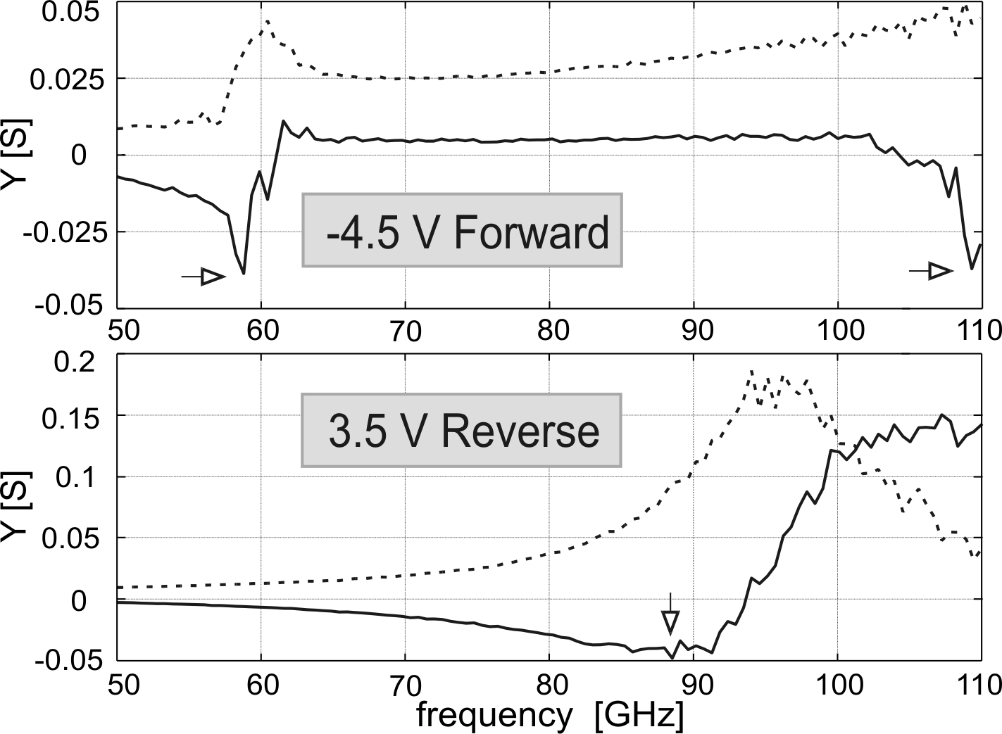
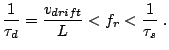
Figure 6.14 shows the admittance of a Gunn diode with the graded gap injector for negative (forward direction) and positive (reverse direction) voltages. The reverse direction looks similar to the one of the diodes without injector. It is not surprising, considering that the injector is designed to work only in the forward direction. For negative voltage, in fact, the influence of the graded gap injector leads to a sharp peak-like appearance of the negative conductance minimum near 60 GHz. The sharp negative conductance minimum is a direct consequence of the dead zone reduction caused by the injector. Additionally, a shift to lower frequencies can be observed and the second harmonic minimum appears.
|
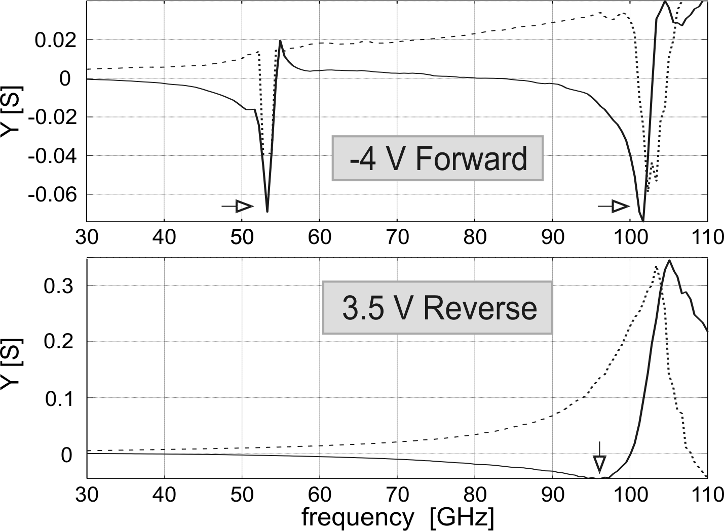
Figure 6.14 shows the admittance of a Gunn diode with the resonant tunneling injector for negative and positive voltages. Again, the reverse direction looks similar to the one of the diodes with the graded gap injector and without injector. In the forward direction, also the resonant tunneling injector presents a peak-like resonance of the negative conductance minimum. The minimum is sharper than for the graded gap injector and the shift to lower frequency is larger. These results represent a further evidence of the significant potentials of the resonant tunneling injector.
On the basis of the Gunn diode small signal admittance (see
section 2.1.4), after McCumber and Heime
[MC66,Hei71]
where the number m accounts for higher harmonics, which can be observed also in Fig. 6.13 in the forward direction, near 110 GHz.
Equation 6.14 can be applied to the measured diodes,
in order to estimate the drift velocity dependance on the electric
field. In Table 6.3, samples with different active
region lengths (
![]() and
and
![]() ) and different areas are compared at
) and different areas are compared at
![]() . The experimental values prove the predictions of
Eq. (6.14): there is an inverse proportionality between the
frequencies of the negative conductance minimum (
. The experimental values prove the predictions of
Eq. (6.14): there is an inverse proportionality between the
frequencies of the negative conductance minimum (
![]() transit time) and the active region length. The value
transit time) and the active region length. The value
![]() can be interpreted as the average group velocity
of the electrons in the active region (
can be interpreted as the average group velocity
of the electrons in the active region (
![]() for diodes with injector).
for diodes with injector).
|
|
|
|||
| Area |
|
|
||
| 396 |
59.4 GHz | 1.06E5 m/s | 69.8 GHz | 1.05E5 m/s |
| 196 |
59.0 GHz | 1.06E5 m/s | 70.8 GHz | 1.06E5 m/s |
| 144 |
62.0 GHz | 1.11E5 m/s | 70.4 GHz | 1.06E5 m/s |
In Gunn diodes the drift velocity depends on three parameters: device temperature, electric field and injector barrier.
The shift with bias to lower frequencies of the negative conductance minima (Fig. 6.12) can be understood thinking on the electric field-drift velocity characteristic for GaAs: the increase of the applied voltage leads to a quasi-proportional change of the electric field, at the same time the drift velocity should decrease (we are considering electric fields higher than the critical electric field).
In Fig. 6.15 the measured drift velocity
(
![]() ) is shown as a function of the supplied voltage.
The diode without injector behaves symmetrically applying positive
and negative biases. For voltages lower than
) is shown as a function of the supplied voltage.
The diode without injector behaves symmetrically applying positive
and negative biases. For voltages lower than
![]() ,
there is no Gunn effect; from
,
there is no Gunn effect; from
![]() up to
up to
![]() , the drift velocity increases and reaches a
maximum; for voltages higher than
, the drift velocity increases and reaches a
maximum; for voltages higher than
![]() , the drift
velocity decreases rapidly.
, the drift
velocity decreases rapidly.
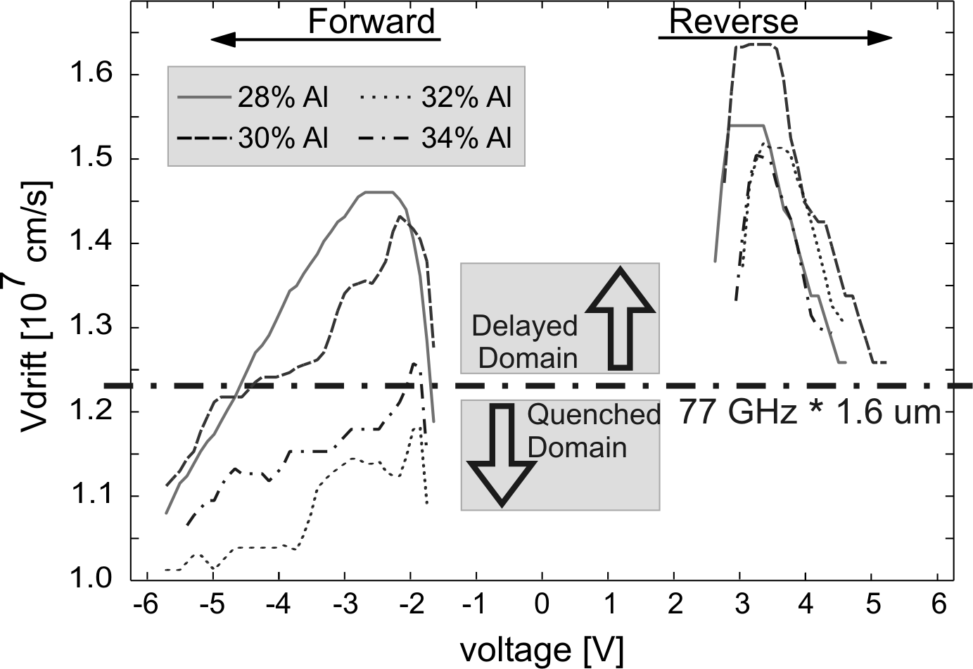
The drift velocity for diodes with injector is asymmetric (Fig. 6.16). In the reverse direction, it can be assumed that there is no injector, since in this configuration the graded gap barrier is situated at the end of the active region. Therefore, the voltage dependance of the drift velocity is very similar to the one without injector. In the forward direction, because of the injector barrier, the electrons are already hot when they enter the active region and the resulting drift velocity is smaller. A clear tendency can be observed as a function of the Al-content in the injector layer: the higher the Al-content, the lower the drift velocity and the flatter the slope of the curve. This property is directly connected with the diode frequency stability. Diodes with flatter drift velocity-voltage dependance should be less affected by temperature or voltage changes, because the occupation of the L-valley is mainly dominated by the hot electron injection rather than the electrical field or temperature activated process.
|
|
A direct, voltage depending comparison between the negative conductance minima of the planar diodes and the oscillating frequencies of the packaged diodes cannot be made. When diodes are mounted inside a resonator, their behavior will be additionally affected by the resonator properties. However, with the help of the planar structures, some important trends in the high frequency behaviors have been identified, leading to a better layer structure and to an optimization of the packaged diodes.
By placing a transferred electron device in a cavity or resonant circuit, we can distinguish three main operational modes (see chapter 2.3.3):
 |
(6.15) |
 |
(6.16) |
 |
(6.17) |
Normally, a Gunn diode cavity oscillator has to be mechanically tuned, in order to get the largest power output at the corresponding desired frequency; comparing this target oscillating frequency with the drift velocity, the oscillating mode of the diode can be determined even before packaging. Different oscillation modes exhibit different powers, efficiencies and thermal stability properties [Hob72,Mak79].
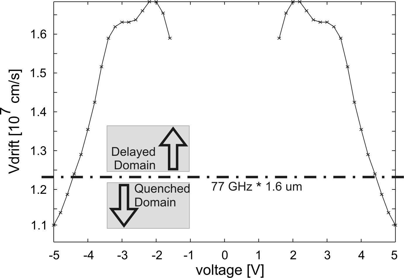
In our case, a frequency of about 77 GHz is required, the active
region is
![]() long and a transit time mode is
expected for drift velocities around
long and a transit time mode is
expected for drift velocities around
![]() .
Drift velocities lower than
.
Drift velocities lower than ![]() correspond to the Quenched
Domain mode, drift velocities higher than
correspond to the Quenched
Domain mode, drift velocities higher than ![]() correspond to the
Delayed Domain mode. Sample with high Al content in the injector
(32% and 34%) can oscillate at 77 GHz only in the Quenched
Domain mode.
correspond to the
Delayed Domain mode. Sample with high Al content in the injector
(32% and 34%) can oscillate at 77 GHz only in the Quenched
Domain mode.
In the case of a second harmonic oscillator, the required frequency is 38.5 GHz and the only operating mode is the Delayed Domain for all the considered structures.
This qualitative analysis, summarized in Fig. 6.15 and 6.16, does not need the complete exact circuit conditions but neglects one important parameter: the domain formation. In fact, the domain formation time and the corresponding dead-zone length can not be easily estimated from small signal measurements. The dead-zone, that is also responsible for temperature instabilities and high noise levels, is dramatically reduced with an optimized hot electron injector.
As seen in Eq. (6.19), the change in ![]() is caused by a
change in the ratio between
is caused by a
change in the ratio between
![]() and
and ![]() . From the I-V
characteristics (low voltages), we expect that the voltage drop on
the injector is not symmetric in the forward and reverse
directions. In order to have a reliable value of the electric
field E in the active region, an accurate computation of the
voltage drop on the injector has to be performed. For this
purpose, results from Silvaco [Int] commercial package
and manual fitting with a load-line model have been compared and
taken into account. From Hall measurements of calibration samples,
the
. From the I-V
characteristics (low voltages), we expect that the voltage drop on
the injector is not symmetric in the forward and reverse
directions. In order to have a reliable value of the electric
field E in the active region, an accurate computation of the
voltage drop on the injector has to be performed. For this
purpose, results from Silvaco [Int] commercial package
and manual fitting with a load-line model have been compared and
taken into account. From Hall measurements of calibration samples,
the ![]() -valley electron mobility has been determined to be
-valley electron mobility has been determined to be
![]() . According to
McCumber (
. According to
McCumber (
![]() [MC66])
and to Hakki (
[MC66])
and to Hakki (
![]() [Hak67]) the
[Hak67]) the ![]() -valley mobility has been assumed 40 times
lower than the
-valley mobility has been assumed 40 times
lower than the ![]() -valley one.
-valley one.
|
Considering
![]() as the carrier concentration in
the active region (
as the carrier concentration in
the active region (
![]() ),
),
![]() can be expressed by:
can be expressed by:
The experimentally determined ratio of the carrier concentration
in the ![]() -valley (
-valley (![]() ) versus the electrical field E is
presented in Fig. 6.17 for the structure with 32%
aluminium content. It can be easily recognized the effectiveness
of the injector, which is responsible for the occupation
difference between the two current directions: this occupation
difference decreases with E as the
) versus the electrical field E is
presented in Fig. 6.17 for the structure with 32%
aluminium content. It can be easily recognized the effectiveness
of the injector, which is responsible for the occupation
difference between the two current directions: this occupation
difference decreases with E as the ![]() -valley carrier
concentration saturates at high electric fields.
-valley carrier
concentration saturates at high electric fields.
|
In this section, temperature dependant S-parameters are analyzed, showing how the Gunn diode hot electron injector influences the domain transit time and the domain creation. In order to change the active layer temperature of the diode, a custom designed heating arrangement was used: the measurements were performed at room temperature with no need to recalibrate the network analyzer. The substrate was in contact with a copper block cooled or heated by a temperature controlled peltier element (for more details see chapter 4.7.1).
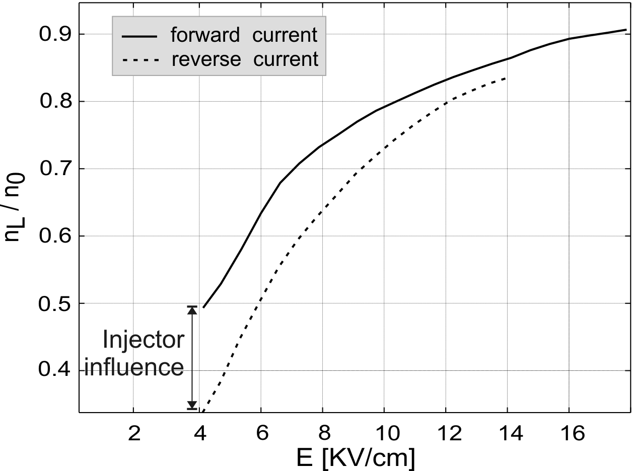
From the measured S-parameters, the temperature dependant drift
velocity has been found as a function of the bias voltage (see
section 6.2.3). As expected, the drift velocity
decreases with increasing temperatures: for the same bias voltage,
at 70
![]()
![]() C the drift velocity is lower than at
0
C the drift velocity is lower than at
0
![]()
![]() C. At 70
C. At 70
![]()
![]() C more electrons
occupy the L-valley, decreasing the average drift velocity. Figure
6.18 shows the described effect for a Gunn
diode with a graded gap injector. Yellow boxes delimit the change
of the drift velocity with the temperature at
C more electrons
occupy the L-valley, decreasing the average drift velocity. Figure
6.18 shows the described effect for a Gunn
diode with a graded gap injector. Yellow boxes delimit the change
of the drift velocity with the temperature at
![]() and
and
![]() . It can be easily noticed, that the box in
the forward current direction is much smaller than the box in the
reverse direction. In other words, the considered diode is more
temperature stable in the forward direction, where the graded gap
injector is designed to work. Moreover, the drift velocity change
with temperature of a Gunn diode with a graded gap injector is
three times less than the one of a Gunn diode without a hot
electron injector.
. It can be easily noticed, that the box in
the forward current direction is much smaller than the box in the
reverse direction. In other words, the considered diode is more
temperature stable in the forward direction, where the graded gap
injector is designed to work. Moreover, the drift velocity change
with temperature of a Gunn diode with a graded gap injector is
three times less than the one of a Gunn diode without a hot
electron injector.
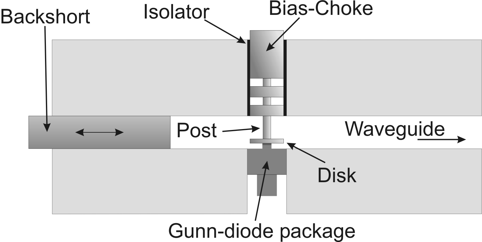
The basic design of a cavity Gunn oscillator is shown in Fig. 6.19. The Gunn diode chip is pressed and fixed on the bottom of the cavity. In this way, the diode is automatically electrically grounded. On the top of the diode, the anode contact is connected to a disk and a post. Changing the diameter of the disk and the length of the post, it is possible to tune respectively a parallel capacitance and a series inductance. The post is combined with a bias choke from which the DC power is provided. The bias choke, which is carefully isolated from the waveguide cavity, is designed as an efficient low-pass filter, in order not to loose any HF power in the DC supply connection. In Fig. 6.19, one can see also a back-short: it is required to mechanically tune the oscillator response. Another adjustable side-short can be moved perpendicular to the cross section plane. The back-short influences strongly the oscillator power and the side-short allows a fine tuning of the frequency.
|
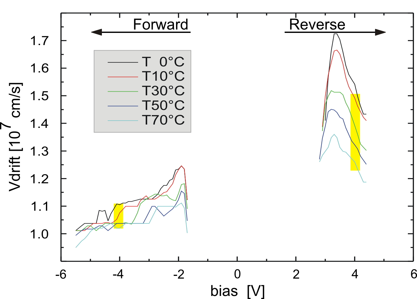
The typical behavior of a second harmonic cavity oscillator is
presented in Fig. 6.20. The oscillator
contains a graded gap injector Gunn diode with a maximum Al
concentration of 32% and a
![]() long GaAs
active region. The frequency and power characteristics versus the
bias voltage have been measured in CW conditions (no pulses). The
Gunn diode starts to oscillate at
long GaAs
active region. The frequency and power characteristics versus the
bias voltage have been measured in CW conditions (no pulses). The
Gunn diode starts to oscillate at
![]() , slightly
after the threshold voltage. The turn on voltage,
, slightly
after the threshold voltage. The turn on voltage, ![]() (the
voltage above the threshold at which coherent RF power is
obtained) can be found around
(the
voltage above the threshold at which coherent RF power is
obtained) can be found around
![]() . Between the
threshold and the turn on voltage, the oscillations are
incoherent. This incoherent regime is not usable; it is similar to
the situation existing in a laser diode before the threshold
current. From 3 to
. Between the
threshold and the turn on voltage, the oscillations are
incoherent. This incoherent regime is not usable; it is similar to
the situation existing in a laser diode before the threshold
current. From 3 to
![]() the frequency increases
monotonically with the bias voltage.
the frequency increases
monotonically with the bias voltage.
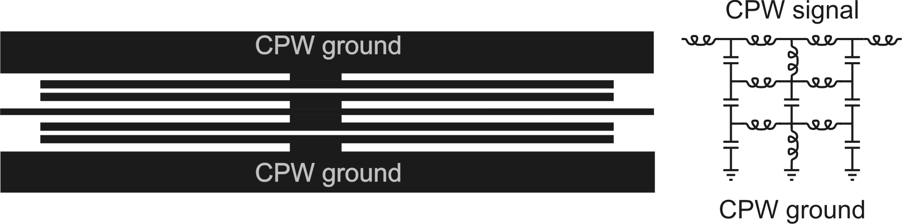
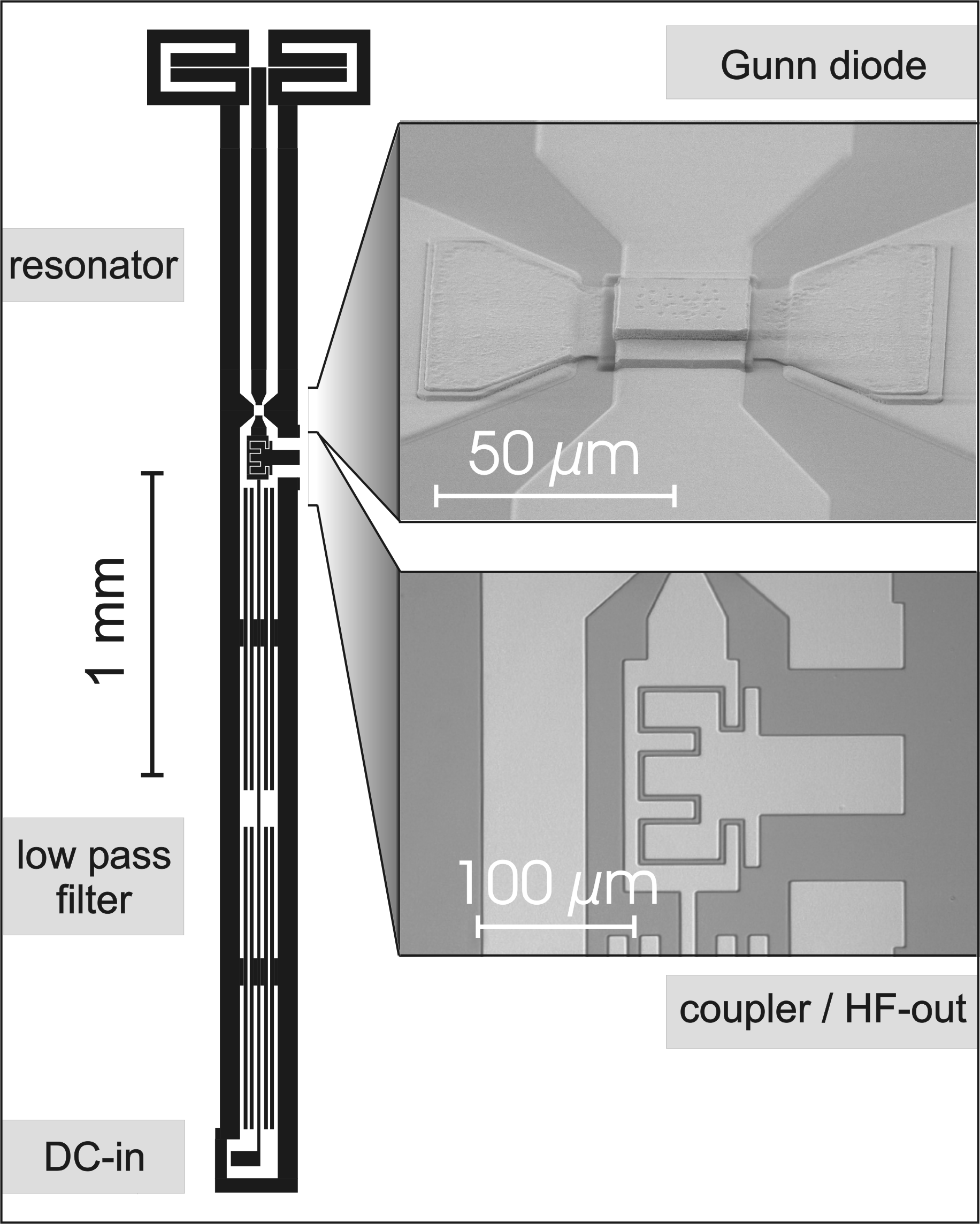
The miniature low-pass filter, used in the MMIC Gunn oscillator, consists in a slow-wave periodic structure proposed by Sor et al. [SQI01]. The main goal is to increase the effective capacitance and inductance along the CPW line. The inductance is enhanced reducing the CPW center conductor width and further capacitances to the ground are created branching out the center conductor and the two grounds. The form of the cell with the equivalent lumped element circuit is illustrated in Fig. 6.21.
Two cell and three cell configurations with
![]() and
and
![]() length per cell respectively, have been
considered. For both of them, the scattering parameters have been
simulated and measured. A detailed description of the measurement
equipment can be found in section 4.7.1. The
low-pass filter has been designed and simulated using Sonnet
Design Suite V.9 [V.903]
length per cell respectively, have been
considered. For both of them, the scattering parameters have been
simulated and measured. A detailed description of the measurement
equipment can be found in section 4.7.1. The
low-pass filter has been designed and simulated using Sonnet
Design Suite V.9 [V.903]
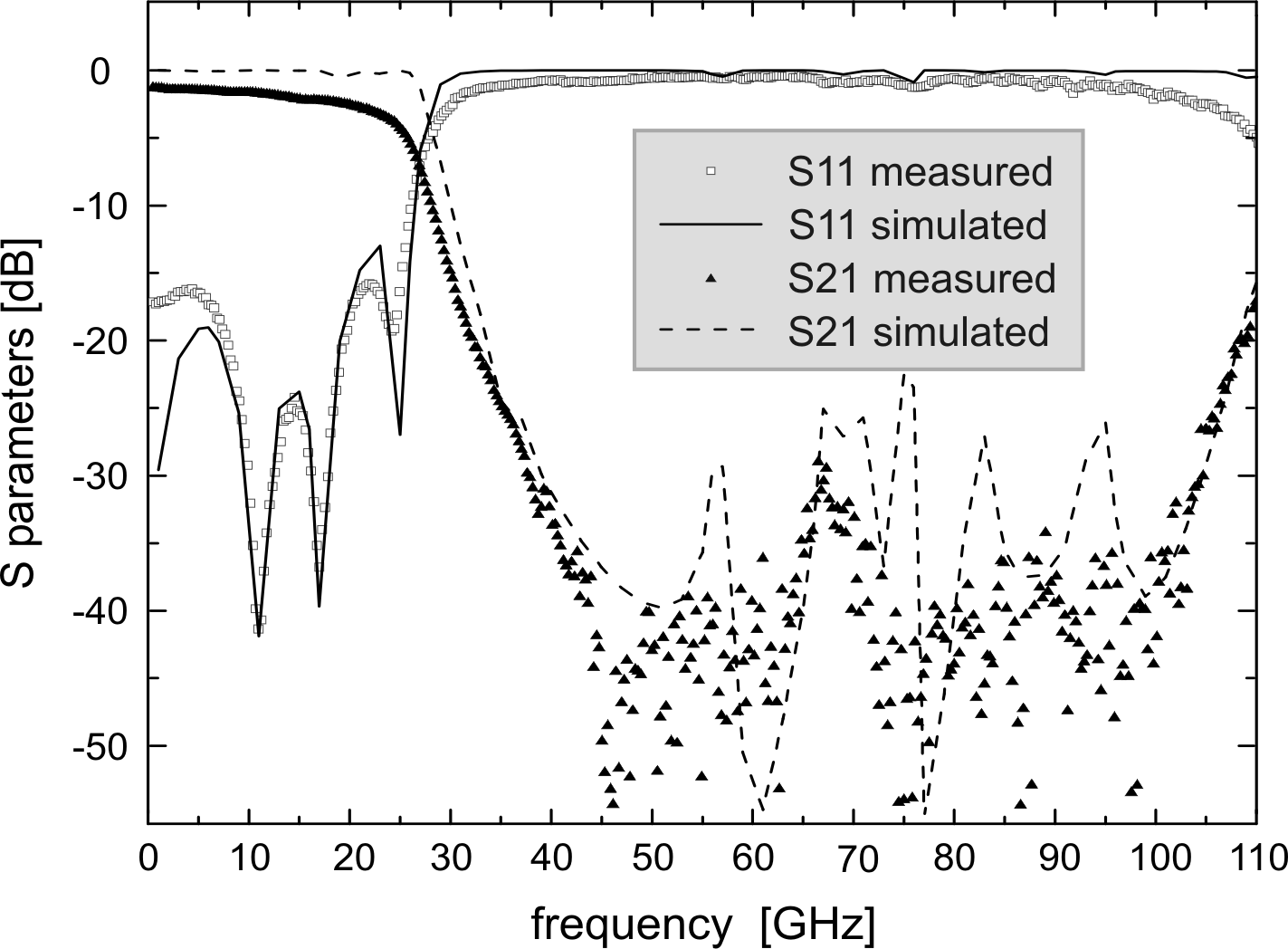
Figure 6.22 shows the response of a periodic
low-pass filter with three
![]() long cells. A good
match between the simulated and experimental S-parameters can be
noticed. The excellent periodic low-pass filter capabilities
demonstrated in [SQI01] have been confirmed. With
long cells. A good
match between the simulated and experimental S-parameters can be
noticed. The excellent periodic low-pass filter capabilities
demonstrated in [SQI01] have been confirmed. With
![]() long cells, the cutoff frequency decreases. This
can be understood considering that, with the same effective
dielectric constant, the cut-off frequency is inverse proportional
to the cell length.
long cells, the cutoff frequency decreases. This
can be understood considering that, with the same effective
dielectric constant, the cut-off frequency is inverse proportional
to the cell length.
|
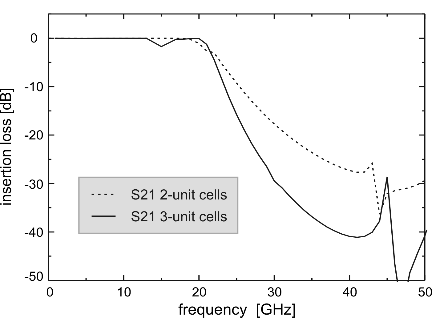
The influence of the cell number is demonstrated in
Fig. 6.23, where two and three cell low-pass filter
are presented. A sharper roll-off can be accomplished simply by
inserting more cells. On the other hand, adding cells can be seen
as a disadvantage, if the integrated circuit size is a priority.
The two cell low-pass filter with
![]() long units
resulted in the best tradeoff between performance and size.
long units
resulted in the best tradeoff between performance and size.
|
In conclusion, the periodic structure has demonstrated a compact size, low insertion losses at low frequencies (pass-band region), high attenuation levels at high frequencies (band-stop region) and a simple filter synthesis and fabrication.
The oscillator design started from DC and S-parameters measurement data of the planar graded gap injector Gunn diode, as described in section 6.2.2.
The oscillating frequency is given by the generalized oscillating condition
|
|
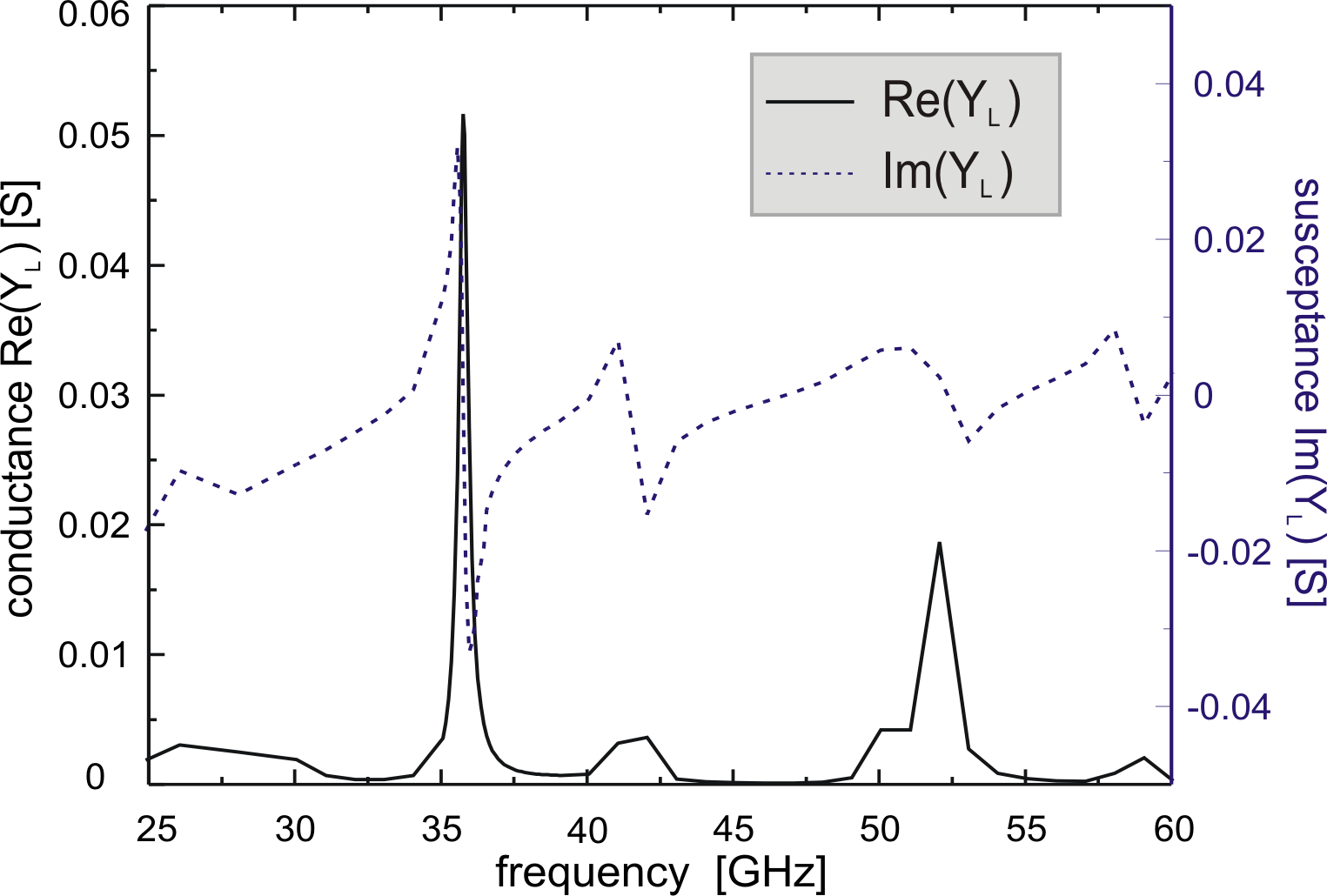
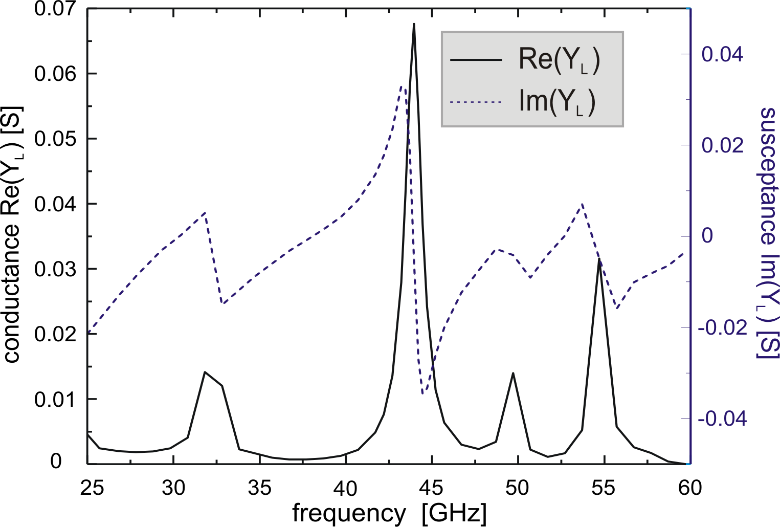
The simulated response of the two considered circuits (at the
diode port) is presented in Fig. 6.25 and in
Fig. 6.26. The first one shows a resonance at
![]() and the second one at
and the second one at
![]() .
The maximum intensity for the conductance is respectively 53 and
.
The maximum intensity for the conductance is respectively 53 and
![]() . Concerning the peak width, the
. Concerning the peak width, the
![]() resonance seems slightly sharper than the
other one.
resonance seems slightly sharper than the
other one.
No direct measurement could confirm the computations: scattering parameters can not be measured in the considered configuration and the required layout change would influence the wave propagation, probably creating artifacts. However, an indirect verification is provided in the next section, where the oscillation frequency for two oscillators based on the described resonant circuits is presented.
The implemented VCO was characterized using wafer probing and a measurement setup composed from a 40-GHz HP8564E spectrum analyzer, two Agilent 11970 (A and U) harmonic mixers and a DPM-2A power meter. The HP-R281A coaxial to waveguide transition connected the picoprobes to the waveguide inputs of the mixers and power meter. As explained in section 6.3.3, two different oscillating circuits have been considered.
In comparison with a cavity Gunn oscillator, the planar one does not require any mechanical tuning: no back-short or side-short are available. Frequency and power characteristics are fixed by the lithographic patterns. If this constitutes a big advantage in a mass production environment, in a research or early development stage, it reduces flexibility and restricts the tolerances for the impedance matching.
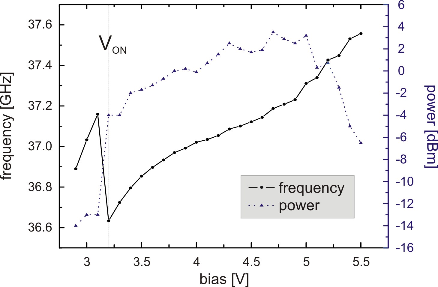
The frequency and the HF output power versus the Gunn diode
tuning voltage of the first oscillator is shown in
Fig. 6.27. After reaching the threshold
voltage, the Gunn diode starts to oscillate. The frequency is not
stable and more peaks can be seen in the spectrum analyzer. At
![]() , we have the so called turn-on voltage
, we have the so called turn-on voltage
![]() . After
. After ![]() , the frequency starts to be stable and
increases monotonously with voltage. The frequency varies from
, the frequency starts to be stable and
increases monotonously with voltage. The frequency varies from
![]() at
at
![]() to
to
![]() at
at
![]() . A typical behavior for a
graded gap injector Gunn diode can be noticed: the turn-on voltage
(
. A typical behavior for a
graded gap injector Gunn diode can be noticed: the turn-on voltage
(
![]() ) is very close to the threshold
(
) is very close to the threshold
(
![]() ). For this reason, a graded gap injector Gunn
diode allows coherent oscillations over a wider voltage range
compared with a standard Gunn diode [NDS+89]. The frequency
characteristics in Fig. 6.27 looks very
similar to the one of the cavity oscillator
(Fig. 6.20). The HF power can be
scaled with the diode diameter and the efficiency is analogous.
). For this reason, a graded gap injector Gunn
diode allows coherent oscillations over a wider voltage range
compared with a standard Gunn diode [NDS+89]. The frequency
characteristics in Fig. 6.27 looks very
similar to the one of the cavity oscillator
(Fig. 6.20). The HF power can be
scaled with the diode diameter and the efficiency is analogous.
|
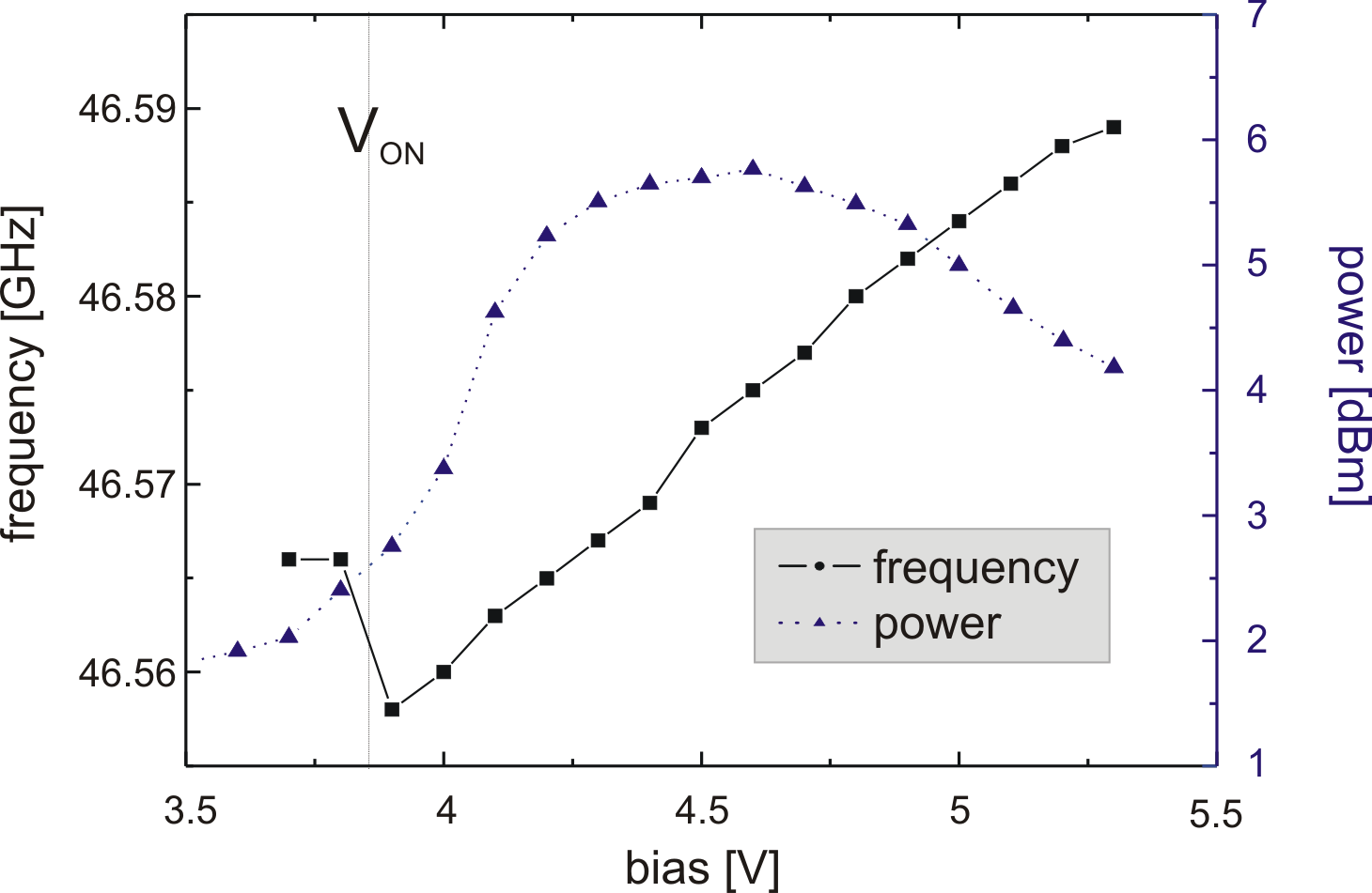
The second planar oscillator with a different resonant circuit is
presented in Fig. 6.28. At
![]() , it generates
, it generates
![]() with a
peak power of
with a
peak power of
![]() . In this second oscillator,
both the power and the frequency are higher than in the first one,
but the voltage tuning of the frequency is inferior. Better tuning
capabilities could be achieved adding to the second circuit a
Schottky varactor.
. In this second oscillator,
both the power and the frequency are higher than in the first one,
but the voltage tuning of the frequency is inferior. Better tuning
capabilities could be achieved adding to the second circuit a
Schottky varactor.
A question remains. Why is the tuning range of the first
oscillator about
![]() and the range of the second
less than
and the range of the second
less than
![]() ? Are the two tuning ranges related
only to the quality factors of the respective resonant circuits?
Actually, an operating mode switch could explain different
pushing6.3 behaviors. In section 6.2.3, a
classification of the operating modes was proposed in connection
to the drift velocity. 37 and
? Are the two tuning ranges related
only to the quality factors of the respective resonant circuits?
Actually, an operating mode switch could explain different
pushing6.3 behaviors. In section 6.2.3, a
classification of the operating modes was proposed in connection
to the drift velocity. 37 and
![]() would correspond
to a velocity of
would correspond
to a velocity of
![]() and
and
![]() ,
respectively. Remembering that all the measured graded gap
injector Gunn diodes had a drift velocity higher than
,
respectively. Remembering that all the measured graded gap
injector Gunn diodes had a drift velocity higher than
![]() , it can be concluded that both the planar oscillators
are operated in the delayed domain mode.
, it can be concluded that both the planar oscillators
are operated in the delayed domain mode.
|
A last consideration: the displayed power levels do not take into account the losses of the picoprobes and of the HF coaxial to waveguide transition. Estimating these losses, we expect that the total output power is with 2dB higher.
simone montanari 2005-08-02